74ALVC16838 Low Voltage 16-Bit Selectable Register/Buffer with 3.6V Tolerant Inputs and Outputs
December 2001
Revised December 2001
74ALVC16838
Low Voltage 16-Bit Selectable Register/Buffer
with 3.6V Tolerant Inputs and Outputs
General Description
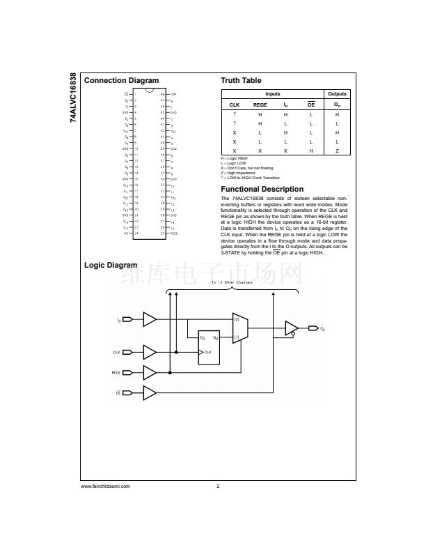
The ALVC16838 contains sixteen non-inverting selectable
buffered or registered paths. The device can be configured
to operate in a registered, or flow through buffer mode by
utilizing the register enable (REGE) and Clock (CLK) sig-
nals. The device operates in a 16-bit word wide mode. All
outputs can be placed into 3-State through use of the OE
Pin. These devices are ideally suited for buffered or regis-
tered 168 pin and 200 pin SDRAM DIMM memory mod-
ules.
The 74ALVC16838 is designed for low voltage (1.65V to
3.6V) V
CC
applications with I/O compatibility up to 3.6V.
The 74ALVC16838 is fabricated with an advanced CMOS
technology to achieve high speed operation while maintain-
ing low CMOS power dissipation.
Features
s
Compatible with PC100 and PC133 DIMM module
specifications
s
1.65V to 3.6V V
CC
supply operation
s
3.6V tolerant inputs and outputs
s
t
PD
(CLK to O
n
)
3.5 ns max for 3.0V to 3.6V V
CC
4.5 ns max for 2.3V to 2.7V V
CC
8.0 ns max for 1.65V to 1.95V V
CC
s
Power-off high impedance inputs and outputs
s
Supports live insertion and withdrawal (Note 1)
s
Uses patented noise/EMI reduction circuitry
s
Ideal for SDRAM DIMM modules
s
Latchup conforms to JEDEC JED78
s
ESD performance:
Human body model
>
2000V
Machine model
>
200V
Note 1:
To ensure the high-impedance state during power up or power
down, OE should be tied to V
CC
through a pull-up resistor; the minimum
value of the resistor is determined by the current-sourcing capability of the
driver.
Ordering Code:
Order Number
74ALVC16838MTD
Package Number
MTD48
Package Description
48-Lead Thin Shrink Small Outline Package (TSSOP), JEDEC MO-153, 6.1mm Wide
Devices also available in Tape and Reel. Specify by appending suffix letter 鈥淴鈥?to the ordering code.
Logic Symbol
Pin Descriptions
Pin Names
OE
I
0
鈥揑
15
O
0
鈥揙
15
CLK
REGE
Description
Output Enable Input (Active LOW)
Inputs
Outputs
Clock Input
Register Enable Input
漏 2001 Fairchild Semiconductor Corporation
DS500714
www.fairchildsemi.com


 1
1
 2
2
 3
3
 4
4
 5
5
 6
6
