74ALVC16374
Low-Voltage 1.8/2.5/3.3 V
16-Bit D-Type Flip-Flop
With 3.6 V鈥揟olerant Inputs and Outputs
(3鈥揝tate, Non鈥揑nverting)
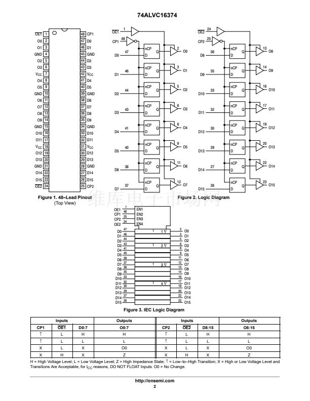
The 74ALVC16374 is an advanced performance, non鈥搃nverting
16鈥揵it D鈥搕ype flip鈥揻lop. It is designed for very high鈥搒peed, very
low鈥損ower operation in 1.8 V, 2.5 V or 3.3 V systems. The
ALVC16374 is byte controlled, with each byte functioning identically,
but independently. Each byte has separate Output Enable and Clock
Pulse inputs. These control pins can be tied together for a full 16鈥揵it
operation.
The 74ALVC16374 consists of 16 edge鈥搕riggered flip鈥揻lops with
individual D鈥搕ype inputs and 3.6 V鈥搕olerant 3鈥搒tate outputs. The
clocks (CPn) and Output Enables (OEn) are common to all flip鈥揻lops
within the respective byte. The flip鈥揻lops will store the state of
individual D inputs that meet the setup and hold time requirements on
the LOW鈥搕o鈥揌IGH Clock (CP) transition. With the OE LOW, the
contents of the flip鈥揻lops are available at the outputs. When the OE is
HIGH, the outputs go to the high impedance state. The OE input level
does not affect the operation of the flip鈥揻lops.
http://onsemi.com
MARKING DIAGRAM
48
48
1
74ALVC16374DT
AWLYYWW
TSSOP鈥?8
DT SUFFIX
CASE 1201
1
= Assembly Location
= Wafer Lot
= Year
= Work Week
A
WL
YY
WW
鈥?/div>
Designed for Low Voltage Operation: V
CC
= 1.65鈥?.6 V
鈥?/div>
3.6 V Tolerant Inputs and Outputs
鈥?/div>
High Speed Operation: 3.6 ns max for 3.0 to 3.6 V
鈥?/div>
鈥?/div>
鈥?/div>
鈥?/div>
鈥?/div>
鈥?/div>
鈥?/div>
4.5 ns max for 2.3 to 2.7 V
7.8 ns max for 1.65 to 1.95 V
Static Drive:
鹵24
mA Drive at 3.0 V
鹵12
mA Drive at 2.3 V
鹵4
mA Drive at 1.65 V
Supports Live Insertion and Withdrawal
I
OFF
Specification Guarantees High Impedance When V
CC
= 0 V
鈥?/div>
Near Zero Static Supply Current in All Three Logic States (40
mA)
Substantially Reduces System Power Requirements
Latchup Performance Exceeds
鹵250
mA @ 125擄C
ESD Performance: Human Body Model >2000 V; Machine Model
>200 V
Second Source to Industry Standard 74ALVC16374
PIN NAMES
Pins
OEn
CPn
D0鈥揇15
O0鈥揙15
Function
Output Enable Inputs
Clock Pulse Inputs
Inputs
Outputs
ORDERING INFORMATION
Device
74ALVC16374DTR
Package
TSSOP
Shipping
2500/Tape & Reel
鈥燭o ensure the outputs activate in the 3鈥搒tate condition, the output enable pins
should be connected to V
CC
through a pull鈥搖p resistor. The value of the resistor is
determined by the current sinking capability of the output connected to the OE pin.
漏
Semiconductor Components Industries, LLC, 2002
1
July, 2002 鈥?Rev. 0
Publication Order Number:
74ALVC16374/D
74ALVC16374/D相關(guān)型號(hào)PDF文件下載
-
型號(hào)
版本
描述
廠商
下載
-
英文版
Quad 2-Input NOR gate
PHILIPS
-
英文版
Quad 2-Input NOR gate
PHILIPS [P...
-
英文版
HEX INVERTERS
TI
-
英文版
Hex Inverter
FAIRCHILD
-
英文版
Hex inverter
PHILIPS
-
英文版
Hex Inverter
FAIRCHILD ...
-
英文版
Hex inverter
PHILIPS [P...
-
英文版
HEX INVERTERS
TI [Texas ...
-
英文版
Quad 2-Input AND gate
PHILIPS
-
英文版
Quad 2-Input AND gate
PHILIPS [N...
-
英文版
QUADRUPLE 2-INPUT POSITIVE-AND GATES WITH OPEN-COLLECTOR OUT...
TI
-
英文版
Quad 2-Input AND Gate with Open Collector Outputs
FAIRCHILD
-
英文版
Quad 2-Input AND Gate with Open Collector Outputs
FAIRCHILD ...
-
英文版
Dual 4-Input NAND gate
PHILIPS
-
英文版
Dual 4-Input NAND gate
PHILIPS [N...
-
英文版
Triple 3-Input NOR gate
PHILIPS
-
英文版
Triple 3-Input NOR gate
PHILIPS [N...
-
英文版
Quad 2-Input OR gate
PHILIPS
-
英文版
Quad 2-Input OR gate
PHILIPS [N...
-
英文版
Quad 2-Input NAND buffer open collector
PHILIPS


 1
1
 2
2
 3
3
 4
4
 5
5
 6
6
 7
7
 8
8
 9
9
 10
10
 11
11
 12
12
