.
.
.
.
.
.
.
.
錚?/div>
= I
OL
= 4 mA (MIN.)
BALANCED PROPAGATION DELAYS
t
PLH
= t
PHL
HIGH NOISE IMMUNITY
V
NIH
= V
NIL
= 28 % V
CC
(MIN.)
WIDE OPERATING VOLTAGE RANGE
V
CC
(OPR) = 2 V TO 6 V
PIN AND FUNCTION COMPATIBLE
WITH 54/74LS194
B1R
(Plastic Package)
F1R
(Ceramic Package)
M1R
(Micro Package)
C1R
(Chip Carrier)
ORDER CODES :
M54HC194F1R
M74HC194M1R
M74HC194B1R
M74HC194C1R
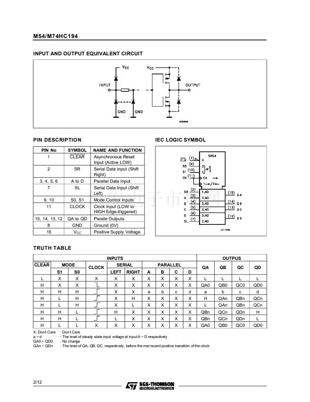
DESCRIPTION
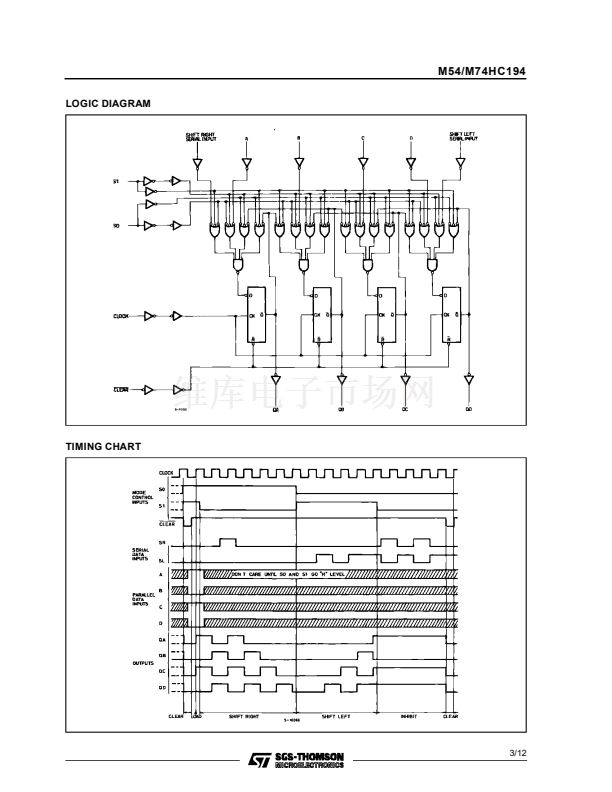
The M54/74HC194 is a high speed CMOS 4 BIT PIPO
2
SHIFT REGISTER fabricated in silicon gate C MOS
technology. It has the same high speed performance
of LSTTL combined with true CMOS low power con-
sumption. This SHIFT REGISTER is designed to in-
corporate virtually all of the features a system designer
may want in a shift register. It features parallel inputs,
parallel outputs, right shift and left shift serial inputs,
clear line. The register has four distinct modes of oper-
ation : PARALLEL (broadside) LOAD ; SHIFT RIGHT
(in the direction Q
A
Q
D
); SHIFT LEFT ; INHIBIT
CLOCK (do nothing). Synchronous parallel loading is
accomplished by applying the four data bits and taking
both mode control inputs, S0 and S1 high. The data
are loaded into their respective flip-flops and appear
at the outputs after the positive transition of the
CLOCK input. During loading, serial data flow is in-
hibited. Shift right is accomplished synchronously with
the rising edge of the clock pulse when S0 is high and
S1 is low. Serial data for this mode is entered at the
SHIFT RIGHT data input. When S0 is low and S1 is
high,data shifts left synchronously and new data is en-
tered at the SHIFT LEFT serial input. Clocking of the
flipflops is inhibited when both mode control inputs are
low. The mode control inputs should be changed only
when the CLOCK input is high. All inputs are equipped
with protection circuits against static discharge and
transient excess voltage.
October 1992
PIN CONNECTIONS
(top view)
NC =
No Internal
Connection
1/12


 1
1
 2
2
 3
3
 4
4
 5
5
 6
6
 7
7
 8
8
 9
9
 10
10
 11
11
 12
12
