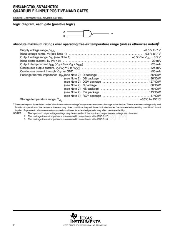
B or Y = A + B in positive logic.
PACKAGE鈥?/div>
QFN 鈥?RGY
PDIP 鈥?N
SOIC 鈥?D
鈥?0擄C to 85擄C
SOP 鈥?NS
SSOP 鈥?DB
TSSOP 鈥?PW
TVSOP 鈥?DGV
CDIP 鈥?J
鈥?5擄C to 125擄C
CFP 鈥?W
LCCC 鈥?FK
Tape and reel
Tube
Tube
Tape and reel
Tape and reel
Tape and reel
Tube
Tape and reel
Tape and reel
Tube
Tube
Tube
ORDERABLE
PART NUMBER
SN74AHCT00RGYR
SN74AHCT00N
SN74AHCT00D
SN74AHCT00DR
SN74AHCT00NSR
SN74AHCT00DBR
SN74AHCT00PW
SN74AHCT00PWR
SN74AHCT00DGVR
SNJ54AHCT00J
SNJ54AHCT00W
SNJ54AHCT00FK
AHCT00
HB00
HB00
HB00
SNJ54AHCT00J
SNJ54AHCT00W
SNJ54AHCT00FK
TOP-SIDE
MARKING
HB00
SN74AHCT00N
AHCT00
鈥?Package drawings, standard packing quantities, thermal data, symbolization, and PCB design guidelines
are available at www.ti.com/sc/package.
FUNCTION TABLE
(each gate)
INPUTS
A
H
L
X
B
H
X
L
OUTPUT
Y
L
H
H
Please be aware that an important notice concerning availability, standard warranty, and use in critical applications of
Texas Instruments semiconductor products and disclaimers thereto appears at the end of this data sheet.
Copyright
錚?/div>
2003, Texas Instruments Incorporated
On products compliant to MIL-PRF-38535, all parameters are tested
unless otherwise noted. On all other products, production
processing does not necessarily include testing of all parameters.
PRODUCTION DATA information is current as of publication date.
Products conform to specifications per the terms of Texas Instruments
standard warranty. Production processing does not necessarily include
testing of all parameters.
POST OFFICE BOX 655303
鈥?/div>
DALLAS, TEXAS 75265
2Y
GND
NC
3Y
3A
1A
1B
1Y
2A
2B
2Y
GND
1
2
3
4
5
6
7
14
13
12
11
10
9
8
V
CC
4B
4A
4Y
3B
3A
3Y
1
14
13
4B
12
4A
11
4Y
10
3B
9
3A
V
CC
1B
1A
NC
V
CC
4B
1Y
NC
2A
NC
2B
4
5
6
7
8
3 2 1 20 19
18
17
16
15
14
9 10 11 12 13
SN54AHCT00 . . . J OR W PACKAGE
SN74AHCT00 . . . D, DB, DGV, N, NS,
OR PW PACKAGE
(TOP VIEW)
SN74AHCT00 . . . RGY PACKAGE
(TOP VIEW)
1B
1Y
2A
2B
2Y
2
3
4
5
6
7
8
4A
NC
4Y
NC
3B
3Y
1


 1
1
 2
2
 3
3
 4
4
 5
5
 6
6
 7
7
 8
8
 9
9
 10
10
 11
11
 12
12
 13
13
 14
14
 15
15
 16
16
 17
17
 18
18
