CD54HC4015, CD74HC4015
Data sheet acquired from Harris Semiconductor
SCHS198C
November 1997 - Revised May 2003
High Speed CMOS Logic
Dual 4-Stage Static Shift Register
Description
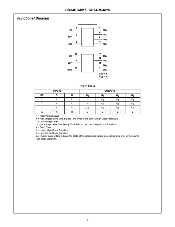
The 鈥橦C4015 consists of two identical, independent, 4-stage
serial-input/parallel-output registers. Each register has
independent Clock (CP) and Reset (MR) inputs as well as a
single serial Data input. 鈥淨鈥?outputs are available from each
of the four stages on both registers. All register stages are D-
type, master-slave 鏗俰p-鏗俹ps. The logic level present at the
Data input is transferred into the 鏗乺st register stage and
shifted over one stage at each positive- going clock
transition. Resetting of all stages is accomplished by a high
level on the reset line.
The device can drive up to 10 low power Schottky equivalent
loads. The 鈥橦C4015 is an enhanced version of equivalent
CMOS types.
Features
[ /Title
(CD74
HC401
5)
/Sub-
ject
(High
Speed
CMOS
Logic
Dual
4-
鈥?Maximum Frequency, Typically 60MHz
C
L
= 15pF, V
CC
= 5V, T
A
= 25
o
C
鈥?Positive-Edge Clocking
鈥?Overriding Reset
鈥?Buffered Inputs and Outputs
鈥?Fanout (Over Temperature Range)
- Standard Outputs . . . . . . . . . . . . . . . 10 LSTTL Loads
- Bus Driver Outputs . . . . . . . . . . . . . 15 LSTTL Loads
鈥?Wide Operating Temperature Range . . . -55
o
C to 125
o
C
鈥?Balanced Propagation Delay and Transition Times
鈥?Signi鏗乧ant Power Reduction Compared to LSTTL
Logic ICs
鈥?HC Types
- 2V to 6V Operation
- High Noise Immunity: N
IL
= 30%, N
IH
= 30% of V
CC
at V
CC
= 5V
Ordering Information
PART NUMBER
CD54HC4015F3A
CD74HC4015E
CD74HC4015M
TEMP. RANGE (
o
C)
-55 to 125
-55 to 125
-55 to 125
PACKAGE
16 Ld CERDIP
16 Ld PDIP
16 Ld SOIC
Pinout
CD54HC4015
(CERDIP)
CD74HC4015
(PDIP, SOIC)
TOP VIEW
2CP 1
2Q
3
2
1Q
2
3
1Q
1
4
1Q
0
5
1MR 6
1D 7
GND 8
16 V
CC
15 2D
14 2MR
13 2Q
0
12 2Q
1
11 2Q
2
10 1Q
3
9 1CP
CAUTION: These devices are sensitive to electrostatic discharge. Users should follow proper IC Handling Procedures.
Copyright
漏
2003, Texas Instruments Incorporated
1


 1
1
 2
2
 3
3
 4
4
 5
5
 6
6
 7
7
 8
8
 9
9
 10
10
