CD54HC221, CD74HC221,
CD74HCT221
Data sheet acquired from Harris Semiconductor
SCHS166F
November 1997 - Revised October 2003
High-Speed CMOS Logic
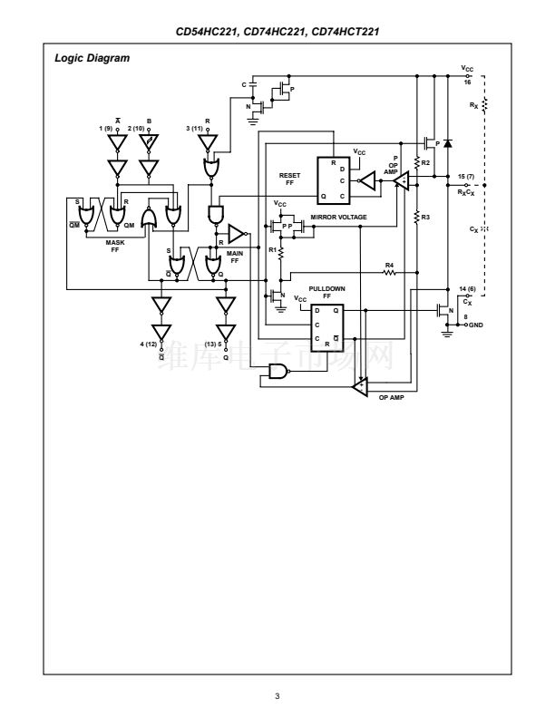
Dual Monostable Multivibrator with Reset
Description
The 鈥橦C221 and CD74HCT221 are dual monostable
multivibrators with reset. An external resistor (R
X
) and an
external capacitor (C
X
) control the timing and the accuracy
for the circuit. Adjustment of R
X
and C
X
provides a wide
range of output pulse widths from the Q and Q terminals.
Pulse triggering on the B input occurs at a particular voltage
level and is not related to the rise and fall time of the trigger
pulse.
Once triggered, the outputs are independent of further trigger
inputs on A and B. The output pulse can be terminated by a
LOW level on the Reset (R) pin. Trailing Edge triggering (A)
and leading-edge-triggering (B) inputs are provided for
triggering from either edge of the input pulse. On power up,
the IC is reset. If either Mono is not used each input (on the
unused device) must be terminated either high or low.
The minimum value of external resistance, R
X
, is typically 500鈩?
The minimum value of external capacitance, C
X
, is 0pF. The
calculation for the pulse width is t
W
= 0.7 R
X
C
X
at V
CC
= 4.5V.
Features
鈥?Overriding RESET Terminates Output Pulse
[ /Title
(CD74
HC221
,
CD74
HCT22
1)
/Sub-
ject
(High
Speed
CMOS
Logic
Dual
Monos
table
Multi-
鈥?Triggering from the Leading or Trailing Edge
鈥?Q and Q Buffered Outputs
鈥?Separate Resets
鈥?Wide Range of Output-Pulse Widths
鈥?Schmitt Trigger on B Inputs
鈥?Fanout (Over Temperature Range)
- Standard Outputs . . . . . . . . . . . . . . . 10 LSTTL Loads
- Bus Driver Outputs . . . . . . . . . . . . . 15 LSTTL Loads
鈥?Wide Operating Temperature Range . . . -55
o
C to 125
o
C
鈥?Balanced Propagation Delay and Transition Times
鈥?Signi鏗乧ant Power Reduction Compared to LSTTL
Logic ICs
鈥?HC Types
- 2V to 6V Operation
- High Noise Immunity: N
IL
= 30%, N
IH
= 30% of V
CC
at V
CC
= 5V
鈥?HCT Types
- 4.5V to 5.5V Operation
- Direct LSTTL Input Logic Compatibility,
V
IL
= 0.8V (Max), V
IH
= 2V (Min)
- CMOS Input Compatibility, I
l
鈮?/div>
1碌A(chǔ) at V
OL
, V
OH
Ordering Information
PART NUMBER
CD54HC221F3A
CD74HC221E
CD74HC221M
CD74HC221MT
CD74HC221M96
TEMP. RANGE (
o
C)
-55 to 125
-55 to 125
-55 to 125
-55 to 125
-55 to 125
-55 to 125
-55 to 125
-55 to 125
-55 to 125
-55 to 125
-55 to 125
-55 to 125
-55 to 125
PACKAGE
16 Ld CERDIP
16 Ld PDIP
16 Ld SOIC
16 Ld SOIC
16 Ld SOIC
16 Ld SOP
16 Ld TSSOP
16 Ld TSSOP
16 Ld TSSOP
16 Ld PDIP
16 Ld SOIC
16 Ld SOIC
16 Ld SOIC
Pinout
CD54HC221
(CERDIP)
CD74HC221
(PDIP, SOIC, SOP, TSSOP)
CD74HCT221
(PDIP, SOIC)
TOP VIEW
1A 1
1B 2
1R 3
1Q 4
2Q 5
2C
X
6
2C
X
R
X
7
GND 8
16 V
CC
15 1C
X
R
X
14 1C
X
13 1Q
12 2Q
11 2R
10 2B
9 2A
CD74HC221NSR
CD74HC221PW
CD74HC221PWR
CD74HC221PWT
CD74HCT221E
CD74HCT221M
CD74HCT221MT
CD74HCT221M96
NOTE: When ordering, use the entire part number. The suf鏗亁es 96
and R denote tape and reel. The suf鏗亁 T denotes a small-quantity
reel of 250.
CAUTION: These devices are sensitive to electrostatic discharge. Users should follow proper IC Handling Procedures.
Copyright
漏
2003, Texas Instruments Incorporated
1


 1
1
 2
2
 3
3
 4
4
 5
5
 6
6
 7
7
 8
8
 9
9
 10
10
 11
11
 12
12
 13
13
 14
14
 15
15
 16
16
 17
17
 18
18
