鈥?/div>
High Capacitive-Drive Capability
鈥睞LS804A
Has Typical Delay Time of 4 ns
(C
L
= 50 pF) and Typical Power Dissipation
of 3.4 mW Per Gate
鈥睞S804B
Has Typical Delay Time of 2.6 ns
(C
L
= 50 pF) and Typical Power Dissipation
of Less Than 9 mW Per Gate
Package Options Include Plastic
Small-Outline (DW) Packages, Ceramic
Chip Carriers (FK), and Standard Plastic (N)
and Ceramic (J) 300-mil DIPs
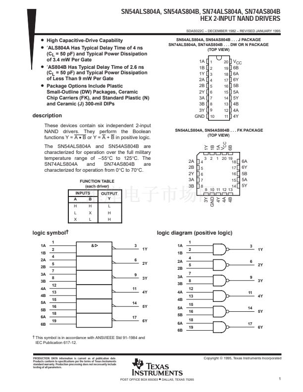
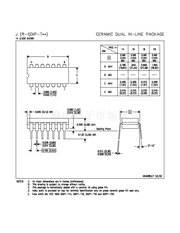
SN54ALS804A, SN54AS804B . . . J PACKAGE
SN74ALS804A, SN74AS804B . . . DW OR N PACKAGE
(TOP VIEW)
description
These devices contain six independent 2-input
NAND drivers. They perform the Boolean
functions Y = A
鈥?/div>
B or Y = A + B in positive logic.
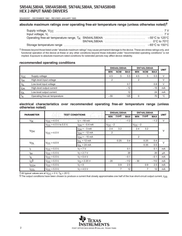
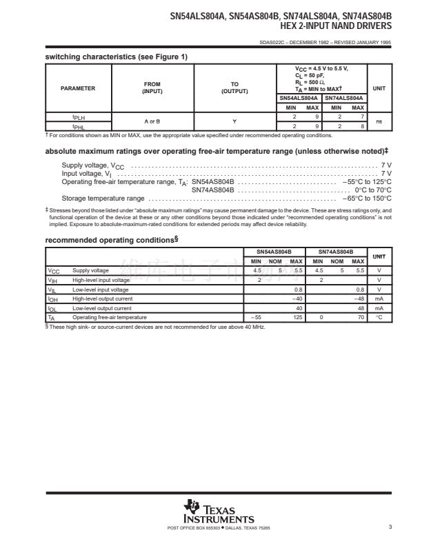
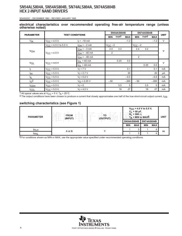
The SN54ALS804A and SN54AS804B are
characterized for operation over the full military
temperature range of 鈥?55擄C to 125擄C. The
SN74ALS804A
and
SN74AS804B
are
characterized for operation from 0擄C to 70擄C.
FUNCTION TABLE
(each driver)
INPUTS
A
H
L
X
B
H
X
L
OUTPUT
Y
L
H
H
1A
1B
1Y
2A
2B
2Y
3A
3B
3Y
GND
1
2
3
4
5
6
7
8
9
10
20
19
18
17
16
15
14
13
12
11
V
CC
6B
6A
6Y
5B
5A
5Y
4B
4A
4Y
SN54ALS804A, SN54AS804B . . . FK PACKAGE
(TOP VIEW)
1Y
1B
1A
V
CC
2A
2B
2Y
3A
3B
4
5
6
7
8
3 2 1 20 19
18
17
16
15
14
9 10 11 12 13
6B
6A
6Y
5B
5A
5Y
logic symbol
鈥?/div>
1A
1B
2A
2B
3A
3B
4A
4B
5A
5B
6A
6B
1
2
4
5
7
8
12
13
15
16
18
19
17
6Y
14
5Y
11
4Y
9
3Y
6
&
3
1Y
logic diagram (positive logic)
1A
1B
2Y
2A
2B
3A
3B
4A
4B
5A
5B
6A
6B
1
2
4
5
7
8
12
13
15
16
18
19
17
6Y
14
5Y
11
4Y
9
3Y
6
2Y
3
1Y
鈥?This symbol is in accordance with ANSI/IEEE Std 91-1984 and
IEC Publication 617-12.
PRODUCTION DATA information is current as of publication date.
Products conform to specifications per the terms of Texas Instruments
standard warranty. Production processing does not necessarily include
testing of all parameters.
Copyright
漏
1995, Texas Instruments Incorporated
POST OFFICE BOX 655303
鈥?/div>
DALLAS, TEXAS 75265
3Y
GND
4Y
4A
4B
1


 1
1
 2
2
 3
3
 4
4
 5
5
 6
6
 7
7
 8
8
 9
9
 10
10
 11
11
 12
12
 13
13
