REVISIONS
LTR
A
DESCRIPTION
Changes in table I: Page 4, input offset voltage should read +V
CC
= 3.5 V,
-V
CC
= -32.5 V. Page 5, gain error, reference subgroups 4, 5, 6, as separate
tests. Temperature limits +V
CC
= 32.5 V should be .06 instead of .02.
Page 6, changes acquisition parameters. Page 10, add replacement military
specification part number. Inactivate drawing for new design.
Editorial changes throughout.
Changes in accordance with N.O.R. 5962-R313-92.
Add generic part number 5537 as device type 02. Add vendor CAGE 18324.
Add case outline letter P. Make changes to 1.2.1, 1.2.2, 1.3, TABLE I, and
FIGURE 1. Redrawn.
Add device class level Q and V devices. Add case outline letter Z. Make
changes to 1.2.2, 1.3, figure 1, table II, and the gain error test as specified in
table I. - ro
DATE (YR-MO-DA)
88-05-11
APPROVED
M. A. FRYE
B
C
92-10-08
94-04-19
M. A. FRYE
M. A. FRYE
D
01-05-25
R. MONNIN
THE ORIGINAL FIRST SHEET OF THIS DRAWING HAS BEEN REPLACED.
REV
SHEET
REV
SHEET
REV STATUS
OF SHEETS
PMIC N/A
D
15
D
16
REV
SHEET
D
1
D
2
D
3
D
4
D
5
D
6
D
7
D
8
D
9
D
10
D
11
D
12
D
13
D
14
PREPARED BY
MARCIA B. KELLEHER
STANDARD
MICROCIRCUIT
DRAWING
THIS DRAWING IS AVAILABLE
FOR USE BY ALL
DEPARTMENTS
AND AGENCIES OF THE
DEPARTMENT OF DEFENSE
CHECKED BY
RAY MONNIN
DEFENSE SUPPLY CENTER COLUMBUS
COLUMBUS, OHIO 43216
http://www.dscc.dla.mil
APPROVED BY
MICHAEL A. FRYE
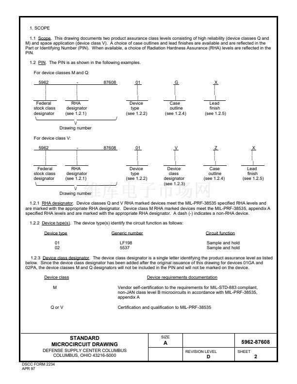
MICROCIRCUIT, LINEAR, SAMPLE AND HOLD,
MONOLITHIC SILICON
DRAWING APPROVAL DATE
87-06-17
AMSC N/A
REVISION LEVEL
D
SIZE
A
SHEET
CAGE CODE
67268
1 OF
16
5962-87608
DSCC FORM 2233
APR 97
DISTRIBUTION STATEMENT A. Approved for public release; distribution is unlimited.
5962-E445-01


 1
1
 2
2
 3
3
 4
4
 5
5
 6
6
 7
7
 8
8
 9
9
 10
10
 11
11
 12
12
 13
13
 14
14
 15
15
 16
16
 17
17
