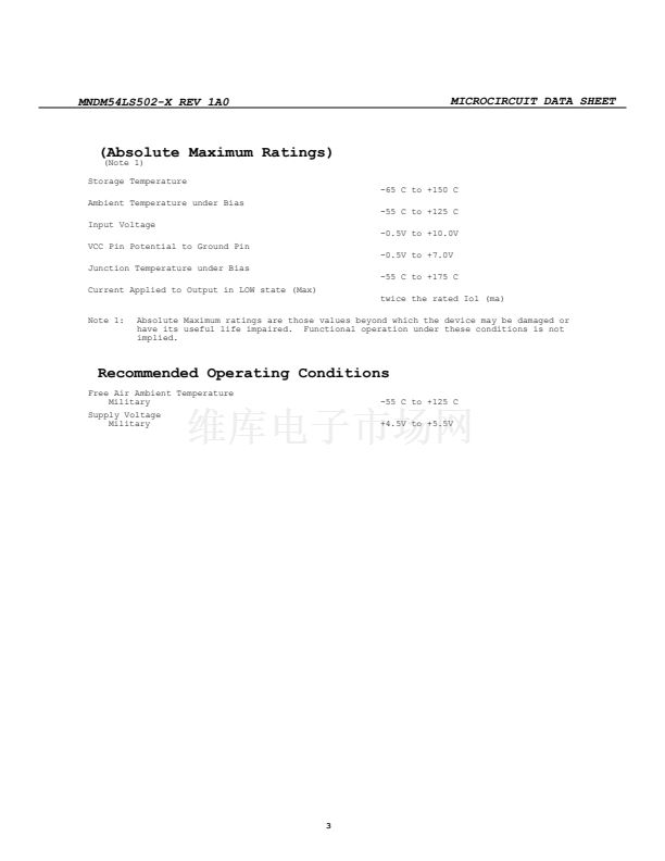
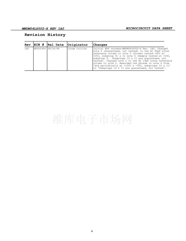
MICROCIRCUIT DATA SHEET
MNDM54LS502-X REV 1A0
Original Creation Date: 04/20/98
Last Update Date: 08/24/98
Last Major Revision Date: 04/20/98
8 - BIT SUCCESSIVE APPROXIMATION REGISTER
General Description
The 'LS502 is an 8-bit register with the interchange logic necessary to perform
serial-to-parallel conversion and provide an active LOW Conversion Complete (CC) signal
coincident with storage of the eighth bit. An active LOW Start (S) input performs
synchronous initialization which forces Q7 LOW and all others HIGH. Subsequent clocks
shift Q7 LOW signal downstream which simultaneously backfills the register such that the
first serial data (D input) bit is stored in Q7, the second bit in Q6, the third in Q5,
etc. The serial input data is also synchronized by an auxilliary flip-flop and brought
out on QD.
Designed primarily for use in the successive approximate technique for analog-to-digital
conversion, the 'LS502 can also be used as a serial-to-parallel conversion ring counter
and as the storage and control element in recursive digital routines.
Industry Part Number
54LS502
NS Part Numbers
DM54LS502J/883*
DM54LS502W/883**
Prime Die
L502
Controlling Document
5962-9080001MEA*, MFA**
Processing
MIL-STD-883, Method 5004
Subgrp Description
1
2
3
4
5
6
7
8A
8B
9
10
11
Static tests at
Static tests at
Static tests at
Dynamic tests at
Dynamic tests at
Dynamic tests at
Functional tests at
Functional tests at
Functional tests at
Switching tests at
Switching tests at
Switching tests at
Temp (
o
C)
+25
+125
-55
+25
+125
-55
+25
+125
-55
+25
+125
-55
Quality Conformance Inspection
MIL-STD-883, Method 5005
1


 1
1
 2
2
 3
3
 4
4
 5
5
 6
6
