MILITARY DATA SHEET
MN54F651-X REV 1A0
TRANSCEIVERS/REGISTERS
General Description
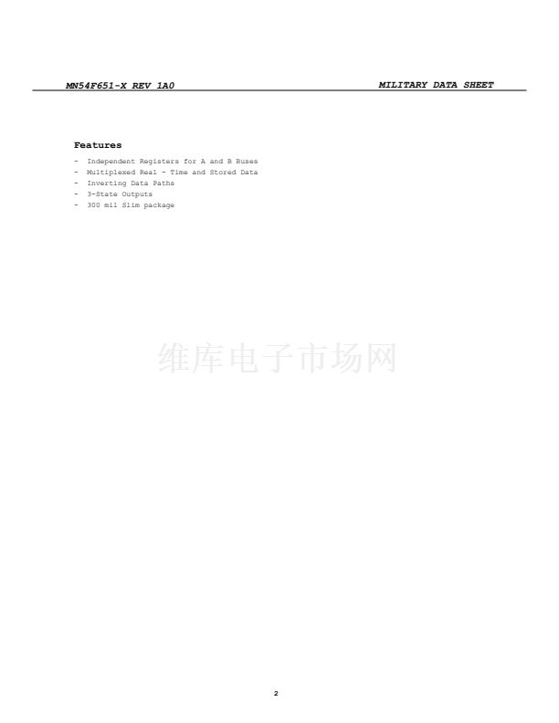
This device consists of bus transceiver circuits with D-type flip-flops, and control
circuitry arranged for multiplexed transmission of data directly from the input bus or
from internal registers. Data on the A or B bus will be clocked into the registers as the
appropriate clock pin goes to HIGH logic level. Output Enable pins (OEAB, OEBA) are
provided to control the transceiver function.
Original Creation Date: 05/08/96
Last Update Date: 07/30/96
Last Major Revision Date: 05/08/96
Industry Part Number
54F651
NS Part Numbers
54F651DMQB
54F651FMQB
54F651LMQB
Prime Die
M651
Processing
MIL-STD-883, Method 5004
Subgrp Description
1
2
3
4
5
6
7
8A
8B
9
10
11
Static tests at
Static tests at
Static tests at
Dynamic tests at
Dynamic tests at
Dynamic tests at
Functional tests at
Functional tests at
Functional tests at
Switching tests at
Switching tests at
Switching tests at
Temp (
o
C)
+25
+125
-55
+25
+125
-55
+25
+125
-55
+25
+125
-55
Quality Conformance Inspection
MIL-STD-883, Method 5005
1


 1
1
 2
2
 3
3
 4
4
 5
5
 6
6
