鈥?/div>
IN
1 8
VDD
All-silicon, low-power CMOS
O2
2 7
O1
technology
O4
3 6
O3
GND
4 5
O5
TTL/CMOS compatible
inputs and outputs
3D7205Z
Vapor phase, IR and wave
SOIC
(150 Mil)
solderable
Auto-insertable (DIP pkg.)
Low ground bounce noise
Leading- and trailing-edge accuracy
Delay range:
8 through 500ns
Delay tolerance:
5% or 2ns
Temperature stability:
鹵3%
typical (0C-70C)
Vdd stability:
鹵2%
typical (4.75V-5.25V)
Minimum input pulse width:
20% of total delay
14-pin DIP and 16-pin SOIC available as drop-in
replacements for hybrid delay lines
data
3
廬
delay
devices,
inc.
PACKAGES
IN
O2
O4
GND
1
2
3
4
8
7
6
5
VDD
O1
O3
O5
IN
N/C
N/C
O2
N/C
O4
GND
1
2
3
4
5
6
7
14
13
12
11
10
9
8
VDD
N/C
O1
N/C
O3
N/C
O5
3D7205M DIP
3D7205H Gull-Wing
(300 Mil)
IN
N/C
N/C
O2
N/C
O4
N/C
GND
1
2
3
4
5
6
7
8
16
15
14
13
12
11
10
9
VDD
N/C
N/C
O1
N/C
O3
N/C
O5
3D7205 DIP
3D7205G Gull-Wing
3D7205K Unused pins
removed
(300 Mil)
3D7205S SOIC
(300 Mil)
FUNCTIONAL DESCRIPTION
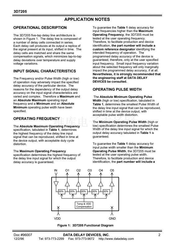
The 3D7205 5-Tap Delay Line product family consists of fixed-delay
CMOS integrated circuits. Each package contains a single delay line,
tapped and buffered at 5 points spaced uniformly in time. Tap-to-tap
(incremental) delay values can range from 8.0ns through 100ns. The
input is reproduced at the outputs without inversion, shifted in time as per
the user-specified dash number. The 3D7205 is TTL- and CMOS-
compatible, capable of driving ten 74LS-type loads, and features both
rising- and falling-edge accuracy.
PIN DESCRIPTIONS
IN
O1
O2
O3
O4
O5
VCC
GND
N/C
Delay Line Input
Tap 1 Output (20%)
Tap 2 Output (40%)
Tap 3 Output (60%)
Tap 4 Output (80%)
Tap 5 Output (100%)
+5 Volts
Ground
No Connection
The all-CMOS 3D7205 integrated circuit has been designed as a reliable,
economic alternative to hybrid TTL fixed delay lines. It is offered in a standard 8-pin auto-insertable DIP
and a space saving surface mount 8-pin SOIC.
TABLE 1: PART NUMBER SPECIFICATIONS
PART NUMBER
DIP-8
3D7205M
3D7205H
SOIC-8
3D7205Z
DIP-14
3D7205
3D7205G
3D7205K
SOIC-16
3D7205S
TOLERANCES
TOTAL
DELAY (ns)
TAP-TAP
DELAY
(ns)
Max
Operating
Frequency
INPUT RESTRICTIONS
Absolute
Max
Oper. Freq.
Min
Operating
Pulse Width
Absolute
Min
Oper. P.W.
-8
-10
-15
-20
-25
-30
-50
-75
-100
NOTE:
-8
-8
-8
9.52 MHz
40.0
鹵
2.0
8.0
鹵
1.5
-10
-10
-10
6.67 MHz
50.0
鹵
2.5
10.0
鹵
2.0
-15
-15
-15
4.44 MHz
75.0
鹵
3.8
15.0
鹵
2.3
-20
-20
-20
3.33 MHz
100
鹵
5.0
20.0
鹵
2.5
-25
-25
-25
2.66 MHz
125
鹵
6.3
25.0
鹵
2.5
-30
-30
-30
2.22 MHz
150
鹵
7.5
30.0
鹵
3.0
-50
-50
-50
1.33 MHz
250
鹵
12.5
50.0
鹵
5.0
-75
-75
-75
0.89 MHz
375
鹵
18.8
75.0
鹵
7.5
-100
-100
-100
0.67 MHz
500
鹵
25.0 100
鹵
10.0
Any dash number between 8 and 100 not shown is also available.
71.4 MHz
50.0 MHz
33.3 MHz
25.0 MHz
20.0 MHz
16.7 MHz
10.0 MHz
6.67 MHz
5.00 MHz
52.5 ns
7.0 ns
75.0 ns
10.0 ns
113 ns
15.0 ns
150 ns
20.0 ns
188 ns
25.0 ns
225 ns
30.0 ns
375 ns
50.0 ns
563 ns
75.0 ns
750 ns
100.0 ns
漏
1996 Data Delay Devices
Doc #96007
12/2/96
DATA DELAY DEVICES, INC.
3 Mt. Prospect Ave. Clifton, NJ 07013
1


 1
1
 2
2
 3
3
 4
4
