錛?/div>
125藲C
10 mA max. (Pin #1= Open or V
IH
)
50渭A max.(Pin #1=V
IL
)
40% to 60% at 50%V
DD
level
5 ns max. (10%V
DD
to 90%V
DD
level)
V
OL
: 10%V
DD
max.
V
OH
: 90%V
DD
min.
15pF max. (CMOS)
150 ns max.
10 ms max.
10 ms max.
鹵5
ppm max.at
錛?5藲C 鹵3藲C
for first year
5pS max.
7pS max.
7pS max.
40pS max.
Deterministic jitter
Random jitter
Norm 1-sigma
Peak to peak
錛?40藲C鹵5藲C
for 10 seconds
錛?50藲C鹵10藲C
for 1 to 2 minutes (preheating)
1.7
#1
3.0
1.7
#2
0.05
1.2
1.5
#4
#3
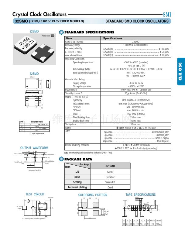
PIN
1
2
3
4
CONNECTION
"L"
OPEN or "H"
GND
Z
OUTPUT
V
DD
Z: high impedance
0.05 1.2
Reflow soldering condition
OUTPUT WAVEFORM
TR
V
OH
("1"Level)
TF
V
DD
90% or 80% V
DD
50% V
DD
V
OL
("0"Level)
GND
10% or 20% V
DD
OV DC
T
Symmetry=t/T 100(%)
脳
(鈥?
Internal crystal oscillation to be halted (Pin#1=V
IL
).
PACKAGE DATA
Item
Lid
Base
Sealing
Terminal plating
Package
t
32SMO
Metal
Ceramic
Seam/EB
Gold
TEST CIRCUIT
Test Point
V
DD
A
#4
V
DD
SOLDERING PATTERN
1.3
1.0
1.3
1.1
TAPE SPECIFICATIONS
4.0鹵0.1
0.1
蠁
1.5
+-
0
1.75鹵0.1
L
2.0鹵0.1
#3
OUTPUT
GND
0.01
渭F鈭?.1
渭F
E/D SW
#1
#2
0.8
DC Power
Supply
0.01渭F
鈭?/div>
0.1渭F
M
B
F
A
V
CL
D
TRI-STATE
1.1
J
CL : including fixture and probe capacitance.
2.3
A
B
C
D
F
J
L
M Reel Dia. Qty/Reel
178
1000pcs
3.5 2.8 8.0 3.5 4.0 1.0 0.3 1.4
C
CLK OSC
-10藲C to
錛?/div>
70藲C (standard)
-40藲C to
錛?/div>
85藲C (W)
錛?/div>
2.5V DC
鹵
0.2V,
32SMO相關(guān)型號(hào)PDF文件下載


 1
1
