鈻?/div>
Electrical Characteristics
T
C
=
25擄C
鹵
3擄C
Parameter
Gate-drain surrender voltage
Diode forward voltage
Gate threshold voltage
Drain-source cutoff current
Gate-source cutoff currentt
Drain-source on resistance
Forward transfer admittance
Short-circuit forward transfer capacitance
(Common-source)
Short-circuit output capacitance
(Common-source)
Reverse transfer capacitance
(Common-source)
Turn-on delay time
Rise time
Turn-off delay time
Fall time
Reverse recovery time
Reverse recovery charge
Symbol
V
DSS
V
DSF
V
th
I
DSS
I
GSS
R
DS(on)
錚碮
fs
錚?/div>
C
iss
C
oss
C
rss
t
d(on)
t
r
t
d(off)
t
f
t
rr
Q
rr
L
=
230
碌H,
V
DD
=
100 V
I
DR
=
15 A, di /dt
=
100 A/
碌s
V
DD
鈮?/div>
100 V, I
D
= 15 A
R
L
鈮?/div>
6.7
鈩?
V
GS
= 10 V
Conditions
I
D
=
1 mA, V
GS
=
0
I
DR
=
30 A, V
GS
=
0
V
DS
=
25 V, I
D
=
1 mA
V
DS
=
184 V, V
GS
=
0
V
GS
= 鹵30
V, V
DS
=
0
V
GS
=
10 V, I
D
=
15 A
V
DS
=
25 V, I
D
=
15 A
V
DS
=
25 V, V
GS
=
0, f
=
1 MHz
8
2
Min
230
Typ
Max
鈭?.5
4
100
鹵1
1.5
鹵0.3
Unit
V
V
V
碌A(chǔ)
碌A(chǔ)
m鈩?/div>
S
pF
pF
pF
ns
ns
ns
ns
ns
nC
55
19
2 330
356
44
39
37
221
46
164
853
74
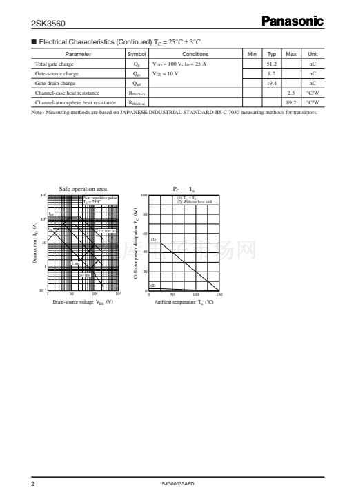
Note) Measuring methods are based on JAPANESE INDUSTRIAL STANDARD JIS C 7030 measuring methods for transistors.
Publication date: February 2004
SJG00033AED
1


 1
1
 2
2
 3
3
