2SK3537-01MR
FUJI POWER MOSFET
N-CHANNEL SILICON POWER MOSFET
Outline Drawings
TO-220F
Super FAP-G Series
Features
High speed switching
Low on-resistance
No secondary breadown
Low driving power
Avalanche-proof
Applications
Switching regulators
UPS (Uninterruptible Power Supply)
DC-DC converters
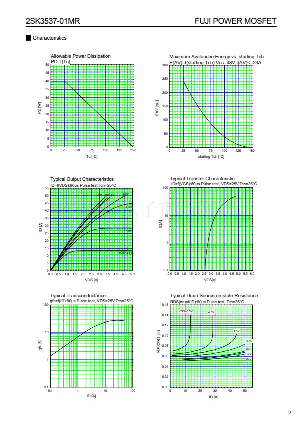
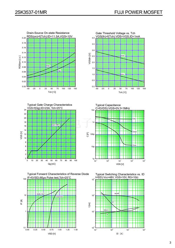
Maximum ratings and characteristic
Absolute maximum ratings
(Tc=25擄C unless otherwise specified)
Item
Drain-source voltage
Continuous drain current
Pulsed drain current
Gate-source voltage
Repetitive or non-repetitive
Maximum Avalanche Energy
Maximum Drain-Source dV/dt
Peak Diode Recovery dV/dt
Max. power dissipation
Operating and storage
temperature range
Symbol
V
DS
V
DSX *5
I
D
I
D(puls]
V
GS
I
AR *2
E
AS *1
dV
DS
/dt
*4
dV/dt
*3
P
D
Ta=25擄C
Tc=25擄C
T
ch
T
stg
Ratings
150
130
鹵23
鹵96
鹵20
23
242
20
5
2.1
40
+150
-55 to +150
Unit
V
V
A
A
V
A
mJ
kV/碌s
kV/碌s
W
擄C
擄C
Equivalent circuit schematic
Drain(D)
Gate(G)
Source(S)
<
<
<
*1 L=0.67mH, Vcc=48V *2 Tch=150擄C *3 I
F
<
D
, -di/dt=50A/碌s, Vcc=BV
DSS
, Tch=150擄C
=-I
*4 V
DS
<150V *5 V
GS
=-20V
=
Electrical characteristics (T
c
=25擄C unless otherwise specified)
Item
Drain-source breakdown voltaget
Gate threshold voltage
Zero gate voltage drain current
Gate-source leakage current
Drain-source on-state resistance
Symbol
V
(BR)DSS
V
GS(th)
I
DSS
I
GSS
R
DS(on)
Test Conditions
I
D
=250碌A(chǔ)
V
GS
=0V
碌A(chǔ)
I
D
= 250
V
DS
=V
GS
V
DS
=150V V
GS
=0V
V
DS
=120V V
GS
=0V
V
GS
=鹵20V V
DS
=0V
I
D
=6A
T
ch
=25擄C
T
ch
=125擄C
V
GS
=4V
V
GS
=5V
V
GS
=10V
12
10
65
60
54
24
1900
200
17
10
15
80
15
46
8
12.5
1.10
0.13
0.6
Min.
150
3.0
Typ.
Max.
5.0
25
250
100
90
81
70
2850
300
26
15
23
120
23
70
12
19
1.65
Units
V
V
碌A(chǔ)
nA
m鈩?/div>
Forward transcondutance
Input capacitance
Output capacitance
Reverse transfer capacitance
Turn-on time t
on
Turn-off time t
off
Total Gate Charge
Gate-Source Charge
Gate-Drain Charge
Avalanche capability
Diode forward on-voltage
Reverse recovery time
Reverse recovery charge
g
fs
C
iss
C
oss
C
rss
td
(on)
t
r
td
(off)
t
f
Q
G
Q
GS
Q
GD
I
AV
V
SD
t
rr
Q
rr
I
D
=11.5A V
DS
=25V
V
DS
=75V
V
GS
=0V
f=1MHz
V
CC
=48V I
D
=11.5A
V
GS
=10V
R
GS
=10
鈩?/div>
V
CC
=48V
I
D
=23A
V
GS
=10V
L=100碌H T
ch
=25擄C
I
F
=23A V
GS
=0V T
ch
=25擄C
I
F
=23A V
GS
=0V
-di/dt=100A/碌s T
ch
=25擄C
S
pF
ns
nC
23
A
V
碌s
碌C
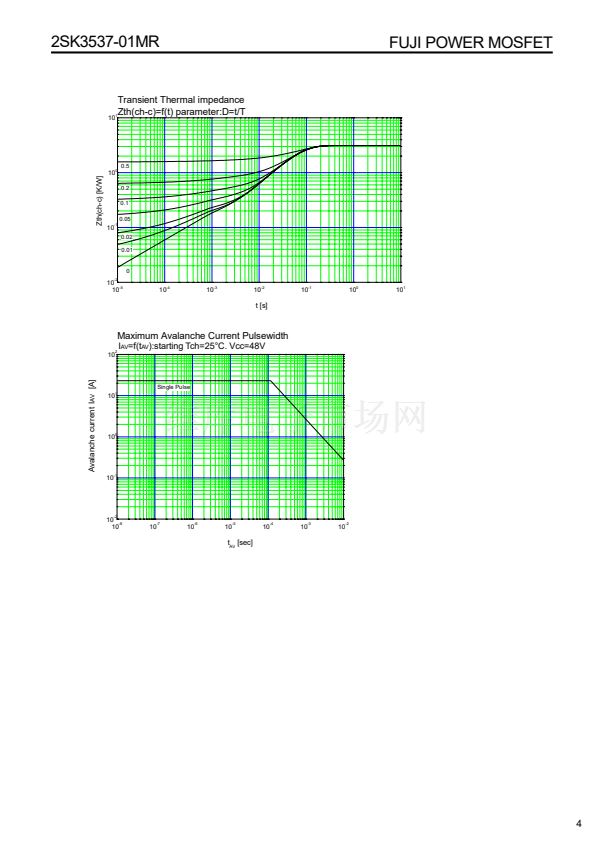
Thermalcharacteristics
Item
Thermal resistance
Symbol
R
th(ch-c)
R
th(ch-a)
Test Conditions
channel to case
channel to ambient
Min.
Typ.
Max.
3.125
58.0
Units
擄C/W
擄C/W
1


 1
1
 2
2
 3
3
 4
4
