2SK3441
TOSHIBA Field Effect Transistor Silicon N Channel MOS Type (U-MOSII)
2SK3441
DC-DC Converter
Relay Drive and Motor Drive Applications
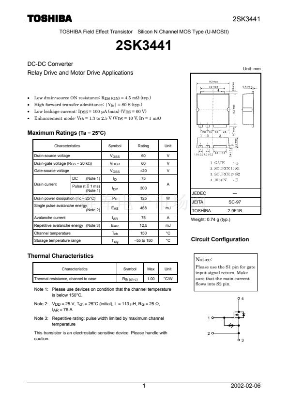
Unit: mm
路
路
路
路
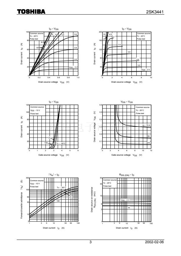
Low drain-source ON resistance: R
DS (ON)
= 4.5 m鈩?(typ.)
High forward transfer admittance: |Y
fs
| = 80 S (typ.)
Low leakage current: I
DSS
=
100
碌A(chǔ) (max) (V
DS
= 60 V)
Enhancement-mode: V
th
=
1.3
to 2.5 V (V
DS
=
10
V, I
D
=
1
mA)
Maximum Ratings
(Ta
=
25擄C)
Characteristics
Drain-source voltage
Drain-gate voltage (R
GS
=
20 kW)
Gate-source voltage
DC
Drain current
(Note 1)
Pulse (t
<
1 ms)
=
(Note 1)
Symbol
V
DSS
V
DGR
V
GSS
I
D
I
DP
P
D
E
AS
I
AR
E
AR
T
ch
T
stg
Rating
60
60
鹵20
75
300
125
468
75
12.5
150
-55
to 150
A
Unit
V
V
V
Drain power dissipation (Tc
=
25擄C)
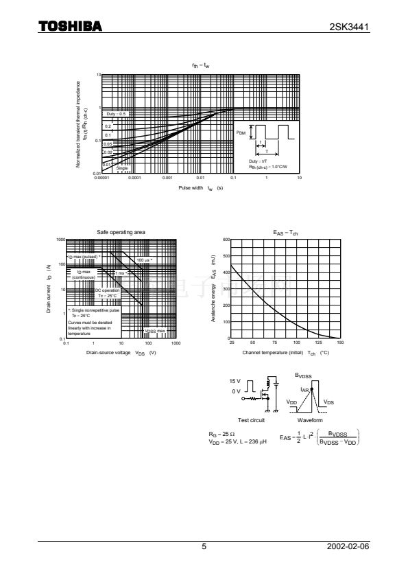
Single pulse avalanche energy
(Note 2)
Avalanche current
Repetitive avalanche energy (Note 3)
Channel temperature
Storage temperature range
JEDEC
W
mJ
A
mJ
擄C
擄C
鈥?/div>
SC-97
2-9F1B
JEITA
TOSHIBA
Weight: 0.74 g (typ.)
Circuit Configuration
Notice:
Thermal Characteristics
Characteristics
Thermal resistance, channel to case
Symbol
R
th (ch-c)
Max
1.00
Unit
擄C/W
Please use the S1 pin for gate
input signal return. Make
sure that the main current
flows into S2 pin.
4
Note 1: Please use devices on condition that the channel temperature
is below 150擄C.
Note 2: V
DD
=
25 V, T
ch
=
25擄C (initial), L
=
113
mH,
R
G
=
25
W,
I
AR
=
75 A
Note 3: Repetitive rating: pulse width limited by maximum channel
temperature
This transistor is an electrostatic sensitive device. Please handle with
caution.
1
2
3
1
2002-02-06


 1
1
 2
2
 3
3
 4
4
 5
5
 6
6
