Power F-MOS FETs
2SK2660
Silicon N-Channel Power F-MOS FET
s
Features
q
High-speed switching
q
High drain-source voltage
6.5鹵0.1
5.3鹵0.1
4.35鹵0.1
unit: mm
2.3鹵0.1
0.5鹵0.1
s
Applications
7.3鹵0.1
1.8鹵0.1
q
High-speed switching
2.5鹵0.1
0.8max
Parameter
Drain to Source breakdown voltage
Gate to Source voltage
Drain current
Allowable power
dissipation
Channel temperature
Storage temperature
DC
Pulse
T
C
= 25擄C
Ta = 25擄C
Symbol
V
DSS
V
GSS
I
D
I
DP
P
D
T
ch
T
stg
Ratings
200
鹵30
鹵4
鹵8
10
1
150
鈭?5
to +150
Unit
V
V
A
A
W
擄C
擄C
0.93鹵0.1
1.0鹵0.1
0.1鹵0.05
0.5鹵0.1
0.75鹵0.1
2.3鹵0.1
4.6鹵0.1
1
2
3
1: Gate
2: Drain
3: Source
U Type Package
s
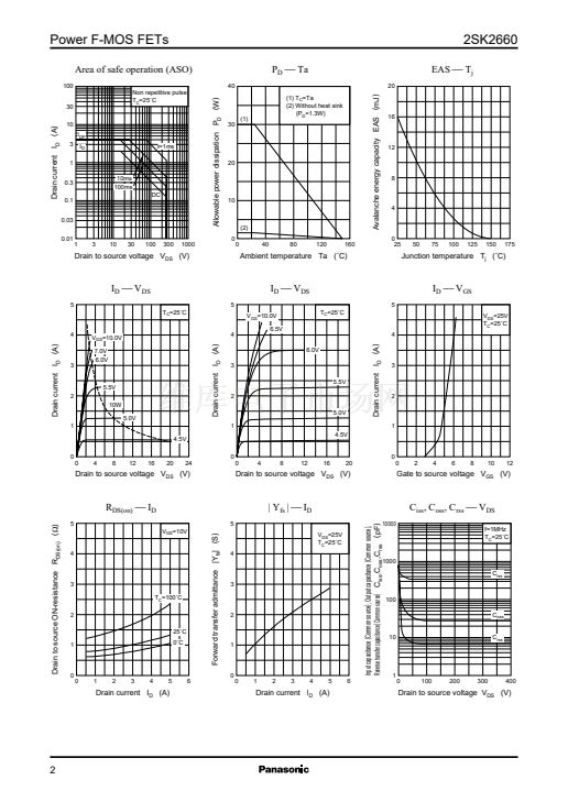
Electrical Characteristics
(T
C
= 25擄C)
Parameter
Drain to Source cut-off current
Gate to Source leakage current
Drain to Source breakdown voltage
Gate threshold voltage
Drain to Source ON-resistance
Forward transfer admittance
Symbol
I
DSS
I
GSS
V
DSS
V
th
R
DS(on)
| Y
fs
|
C
oss
t
d(on)
t
r
t
d(off)
t
f
V
GS
= 10V, I
D
= 2A
R
L
= 50鈩? V
DD
= 100V
Conditions
V
DS
= 160V, V
GS
= 0
V
GS
= 鹵30V, V
DS
= 0
I
D
= 1mA, V
GS
= 0
V
DS
= 25V, I
D
= 1mA
V
GS
= 10V, I
D
= 2A
V
DS
= 25V, I
D
= 2A, f = 1MHz
V
DS
= 20V, V
GS
= 0, f = 1MHz
0.5
200
1
0.8
1
290
50
9
10
25
45
40
5
1.1
min
typ
max
0.1
鹵1
Unit
mA
碌A(chǔ)
V
V
鈩?/div>
S
pF
pF
pF
ns
ns
ns
ns
Input capacitance (Common Source) C
iss
Output capacitance (Common Source)
Reverse transfer capacitance (Common Source) C
rss
Turn-on time (delay time)
Rise time
Turn-off time (delay time)
Fall time
1.0鹵0.2
s
Absolute Maximum Ratings
(T
C
= 25擄C)
1


 1
1
 2
2
