Power F-MOS FETs
2SK1406
Silicon N-Channel Power F-MOS FET
s
Features
q
Low ON-resistance R
DS(on)
: R
DS(on)
= 0.32鈩?(typ.)
q
High-speed switching: t
f
= 140ns (typ.)
q
No secondary breakdown
q
High breakdown voltage, large allowable power dissipation
unit: mm
15.0鹵0.3
11.0鹵0.2
5.0鹵0.2
3.2
0.7
s
Applications
q
Contactless relay
q
Diving circuit for a solenoid
q
Driving circuit for a motor
q
Control equipment
q
Switching power supply
21.0鹵0.5
15.0鹵0.2
蠁3.2鹵0.1
16.2鹵0.5
12.5
3.5
Solder Dip
2.0鹵0.2
2.0鹵0.1
1.1鹵0.1
5.45鹵0.3
10.9鹵0.5
0.6鹵0.2
s
Absolute Maximum Ratings
(T
C
= 25擄C)
Parameter
Drain to Source breakdown voltage
Gate to Source voltage
Drain current
Allowable power
dissipation
Channel temperature
Storage temperature
DC
Pulse
T
C
= 25擄C
Ta = 25擄C
Symbol
V
DSS
V
GSS
I
D
I
DP
P
D
T
ch
T
stg
Ratings
500
鹵20
鹵20
鹵40
100
3
150
鈭?5
to +150
Unit
V
V
A
A
W
擄C
擄C
1
2
3
1: Gate
2: Drain
3: Source
TOP-3 Full Pack Package (a)
s
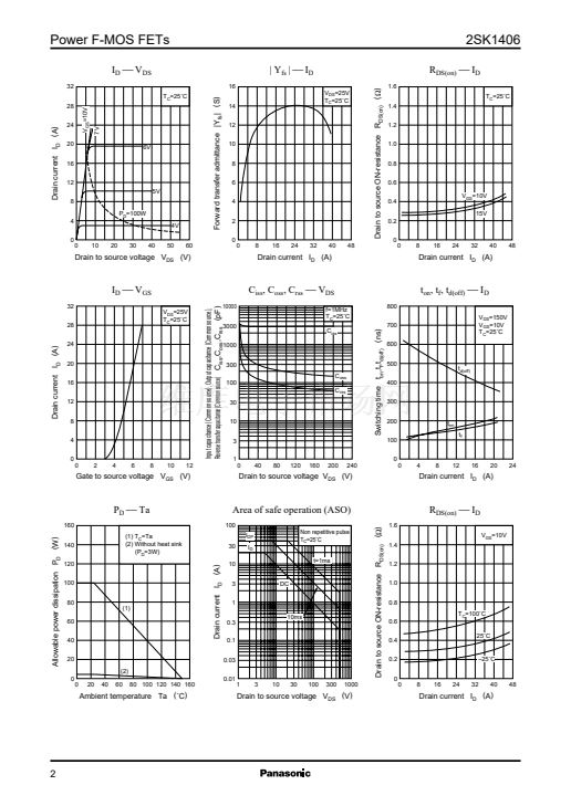
Electrical Characteristics
(T
C
= 25擄C)
Parameter
Drain to Source cut-off current
Gate to Source leakage current
Drain to Source breakdown voltage
Gate threshold voltage
Drain to Source ON-resistance
Drain to Source ON-voltage
Forward transfer admittance
Symbol
I
DSS
I
GSS
V
DSS
V
th
R
DS(on)
V
DS(on)
| Y
fs
|
C
oss
t
on
t
f
t
d(off)
Conditions
V
DS
= 400V, V
GS
= 0
V
GS
= 鹵20V, V
DS
= 0
I
D
= 1mA, V
GS
= 0
V
DS
= 25V, I
D
= 1mA
V
GS
= 10V, I
D
= 10A
V
GS
= 10V, I
D
= 20A
V
DS
= 25V, I
D
= 10A
V
DS
= 20V, V
GS
= 0, f = 1MHz
7.2
12
3000
430
175
V
GS
= 10V, I
D
= 10A
V
DS
= 150V, R
L
= 15鈩?/div>
150
140
480
500
1
0.32
5
0.4
9
min
typ
max
0.1
鹵1
Unit
mA
碌A(chǔ)
V
V
鈩?/div>
V
S
pF
pF
pF
ns
ns
ns
Input capacitance (Common Source) C
iss
Output capacitance (Common Source)
Reverse transfer capacitance (Common Source) C
rss
Turn-on time
Fall time
Turn-off time (delay time)
1


 1
1
 2
2
