DATA SHEET
MOS FIELD EFFECT POWER TRANSISTORS
2SJ495
SWITCHING P-CHANNEL POWER MOS FET INDUSTRIAL USE
DESCRIPTION
This product is P-Channel MOS Field Effect Transistor
designed for high current switching applications.
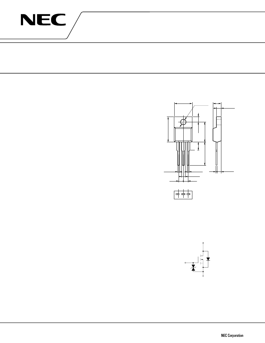
PACKAGE DIMENSIONS
(in millimeter)
10.0 鹵 0.3
3.2 鹵 0.2
4.5 鹵 0.2
2.7 鹵 0.2
FEATURES
鈥?Super Low On-State Resistance
3 鹵 0.1
4 鹵 0.2
R
DS(on)2
= 56 m鈩?MAX. (V
GS
= 鈥? V, I
D
= 鈥?5 A)
鈥?Low C
iss
C
iss
= 4120 pF TYP.
鈥?Built-in Gate Protection Diode
ABSOLUTE MAXIMUM RATINGS (T
A
= 25
擄
C)
Drain to Source Voltage
Gate to Source Voltage*
Gate to Source Voltage
Drain Current (DC)
Drain Current (pulse)**
Total Power Dissipation (T
C
= 25擄C)
Total Power Dissipation (T
A
= 25擄C)
Channel Temperature
Storage Temperature
*f = 20 kHz, Duty Cycle
鈮?/div>
10% (+Side)
**PW
鈮?/div>
10
碌
s, Duty Cycle
鈮?/div>
1%
V
DSS
V
GSS(AC)
V
GSS(DC)
I
D(DC)
I
D(pulse)
P
T
P
T
T
ch
T
stg
鈥?0
m20
鈥?0, 0
m30
m120
35
2.0
150
鈥?5 to +150
V
V
V
A
A
W
W
擄C
擄C
1 2 3
0.7 鹵 0.1
2.54
13.5 MIN.
2.5 鹵 0.1
0.65 鹵 0.1
1. Gate
2. Drain
3. Source
Drain
Body
Diode
Source
1.3 鹵 0.2
1.5 鹵 0.2
2.54
THERMAL RESISTANCE
Channel to Case
Channel to Ambient
R
th(ch-c)
R
th(ch-A)
3.57
62.5
擄C/W
擄C/W
MP-45F (ISOLATED TO-220)
Gate
Gate Protection
Diode
The diode connected between the gate and source of the transistor serves as a protector against ESD. When this deveice
acutally used, an addtional protection circiut is externally required if a voltage exceeding the rated voltage may be applied
to this device.
Document No. D11267EJ2V0DS00 (2nd edition)
Date Published November 1997 N
Printed in Japan
12.0 鹵 0.2
R
DS(on)1
= 30 m鈩?MAX. (V
GS
= 鈥?0 V, I
D
= 鈥?5 A)
15.0 鹵 0.3
漏
1997


 1
1
 2
2
 3
3
 4
4
 5
5
 6
6
 7
7
 8
8
