Silicon Junction FETs (Small Signal)
2SJ0163
(2SJ163)
Silicon P-Channel Junction FET
For general switching
Complementary to 2SK1103
s
Features
q
Low ON-resistance
q
Low-noise characteristics
1
2
(0.95) (0.95)
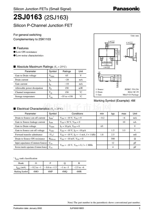
Unit: mm
0.40
+0.10
鈥?.05
3
0.16
+0.10
鈥?.06
1.50
+0.25
鈥?.05
2.8
+0.2
鈥?.3
s
Absolute Maximum Ratings
(T
a
=
25擄C)
Parameter
Gate to Drain voltage
Drain current
Gate current
Allowable power dissipation
Channel temperature
Storage temperature
Symbol
V
GDS
I
D
I
G
P
D
T
ch
T
stg
Ratings
65
鈭?0
鈭?0
150
150
鈭?5
to
+150
Unit
V
mA
mA
mW
擄C
擄C
1: Source
2: Drain
3: Gate
10藲
1.9
鹵0.1
2.90
+0.20
鈥?.05
1.1
+0.2
鈥?.1
(0.65)
0 to 0.1
1.1
+0.3
鈥?.1
JEDEC: TO-236
EIAJ: SC-59
Mini3-G1 Package
Marking Symbol (Example): 4M
s
Electrical Characteristics
(T
a
=
25擄C)
Parameter
Drain to Source cut-off current
Gate to Source leakage current
Gate to Drain voltage
Gate to Source cut-off voltage
Forward transfer admittance
Drain to Source ON-resistance
Symbol
I
DSS*
I
GSS
V
GDS
V
GSC
| Y
fs
|
R
DS(on)
Conditions
V
DS
=
鈭?0
V, V
GS
= 0
V
GS
= 30 V, V
DS
= 0
I
G
= 10
碌A(chǔ),
V
DS
= 0
V
DS
=
鈭?0
V, I
D
=
鈭?0 碌A(chǔ)
V
DS
=
鈭?0
V, I
D
=
鈭?
mA, f = 1 kHz
V
DS
=
鈭?0
mV, V
GS
= 0
V
DS
=
鈭?0
V, V
GS
= 0, f = 1 MHz
1.8
65
1.5
2.5
300
12
4
3.5
min
鈭?/div>
0.2
typ
max
鈭?
10
Unit
mA
nA
V
V
mS
鈩?/div>
pF
pF
Input capacitance (Common Source) C
iss
Reverse transfer capacitance (Common Source) C
rss
*
I
DSS
rank classification
Runk
I
DSS
(mA)
O
鈭?/div>
0.2 to
鈭?
4MO
P
鈭?/div>
0.6 to
鈭?.5
4MP
Q
鈭?
to
鈭?
4MQ
R
鈭?.5
to
鈭?
4MR
Marking Symbol
Note) The part number in the parenthesis shows conventional part number.
Publication date: January 2002
SJF00001BED
0.4
鹵0.2
5藲
1


 1
1
 2
2
 3
3
