Power Transistors
2SD2469, 2SD2469A
Silicon NPN epitaxial planar type
For power switching
Complementary to 2SB1607
Unit: mm
s
Features
q
q
q
q
4.6鹵0.2
蠁3.2鹵0.1
9.9鹵0.3
2.9鹵0.2
4.1鹵0.2 8.0鹵0.2
Solder Dip
Low collector to emitter saturation voltage V
CE(sat)
Satisfactory linearity of foward current transfer ratio h
FE
Large collector current I
C
Full-pack package with outstanding insulation, which can be in-
stalled to the heat sink with one screw
(T
C
=25藲C)
Ratings
130
150
80
100
7
15
7
40
2
150
鈥?5 to +150
Unit
V
15.0鹵0.3
3.0鹵0.2
Parameter
Collector to
base voltage
Collector to
2SD2469
2SD2469A
2SD2469
Symbol
V
CBO
V
CEO
V
EBO
I
CP
I
C
P
C
T
j
T
stg
13.7
鈥?.2
+0.5
s
Absolute Maximum Ratings
1.2鹵0.15
1.45鹵0.15
0.75鹵0.1
2.54鹵0.2
5.08鹵0.4
1 2 3
2.6鹵0.1
0.7鹵0.1
emitter voltage 2SD2469A
Emitter to base voltage
Peak collector current
Collector current
Collector power T
C
=25擄C
dissipation
Ta=25擄C
Junction temperature
Storage temperature
V
V
A
A
W
藲C
藲C
7擄
1:Base
2:Collector
3:Emitter
TO鈥?20E Full Pack Package
s
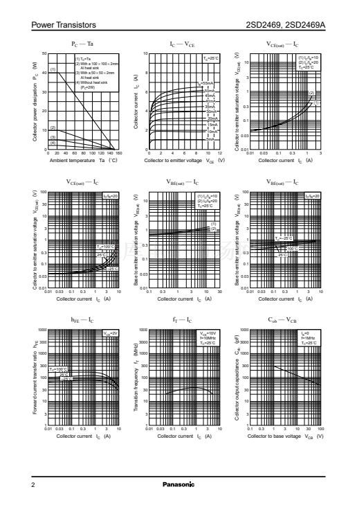
Electrical Characteristics
Parameter
Collector cutoff current
Emitter cutoff current
Collector to emitter
voltage
2SD2469
2SD2469A
(T
C
=25藲C)
Symbol
I
CBO
I
EBO
V
CEO
h
FE1
h
FE2*
V
CE(sat)
V
BE(sat)
f
T
t
on
t
stg
t
f
Conditions
V
CB
= 100V, I
E
= 0
V
EB
= 5V, I
C
= 0
I
C
= 10mA, I
B
= 0
V
CE
= 2V, I
C
= 0.1A
V
CE
= 2V, I
C
= 3A
I
C
= 5A, I
B
= 0.25A
I
C
= 5A, I
B
= 0.25A
V
CE
= 10V, I
C
= 0.5A, f = 10MHz
I
C
= 3A, I
B1
= 0.3A, I
B2
= 鈥?0.3A,
V
CC
= 50V
30
0.5
1.5
0.1
80
100
45
90
260
0.5
1.5
V
V
MHz
碌s
碌s
碌s
min
typ
max
10
50
Unit
碌A(chǔ)
碌A(chǔ)
V
Forward current transfer ratio
Collector to emitter saturation voltage
Base to emitter saturation voltage
Transition frequency
Turn-on time
Storage time
Fall time
*
h
FE2
Rank classification
Q
90 to 180
P
130 to 260
Rank
h
FE2
1


 1
1
 2
2
 3
3
