鈥?/div>
Optimum for the output stage of a Hi-Fi audio amplifier
(3.0)
(1.5)
2.0
鹵0.3
3.0
鹵0.3
1.0
鹵0.2
0.6
鹵0.2
5.45
鹵0.3
10.9
鹵0.5
(1.5)
2.7
鹵0.3
1
2
3
I
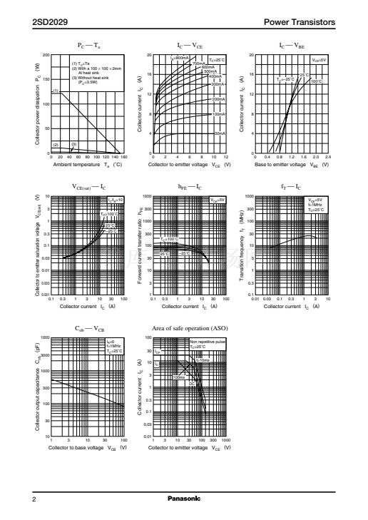
Absolute Maximum Ratings
T
C
=
25擄C
Parameter
Collector to base voltage
Collector to emitter voltage
Emitter to base voltage
Peak collector current
Collector current
Collector power
dissipation
T
C
= 25擄C
T
a
= 25擄C
T
j
T
stg
Symbol
V
CBO
V
CEO
V
EBO
I
CP
I
C
P
C
Rating
160
160
5
20
12
120
3.5
150
鈭?5
to
+150
擄C
擄C
Unit
V
V
V
A
A
W
20.0
鹵0.5
(2.5)
Solder Dip
(1.5)
1: Base
2: Collector
3: Emitter
TOP-3L Package
Junction temperature
Storage temperature
I
Electrical Characteristics
T
C
=
25擄C
Parameter
Collector cutoff current
Emitter cutoff current
Forward current transfer ratio
Symbol
I
CBO
I
EBO
h
FE1
h
FE2 *
h
FE3
Base to emitter voltage
Collector to emitter saturation voltage
Transition frequency
Collector output capacitance
Note) *: Rank classification
Rank
h
FE2
Q
60 to 120
S
80 to 160
P
100 to 200
V
BE
V
CE(sat)
f
T
C
ob
Conditions
V
CB
= 160 V, I
E
= 0
V
EB
= 3 V, I
C
= 0
V
CE
= 5 V, I
C
= 20 mA
V
CE
= 5 V, I
C
= 1 A
V
CE
= 5 V, I
C
= 8 A
V
CE
= 5 V, I
C
= 8 A
I
C
= 8 A, I
B
= 0.8 A
V
CE
= 5 V, I
C
= 0.5 A, f = 1 MHz
V
CB
= 10 V, I
E
= 0, f = 1 MHz
20
210
20
60
20
1.8
2.0
V
V
MHz
pF
200
Min
Typ
Max
50
50
Unit
碌A
碌A
(2.0)
1


 1
1
 2
2
 3
3
 4
4
