printed circuit board, etc. of small electronic equipment
鈻?/div>
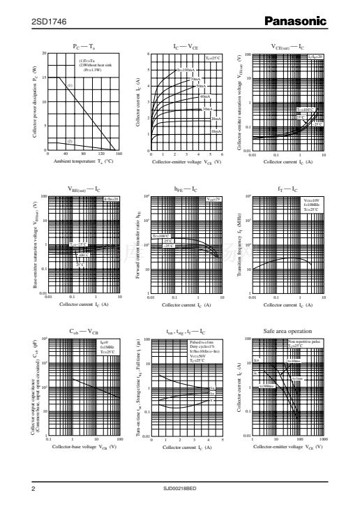
Absolute Maximum Ratings
T
C
=
25擄C
Parameter
Collector-base voltage (Emitter open)
Collector-emitter voltage (Base open)
Emitter-base voltage (Collector open)
Collector current
Peak collector current
Collector power dissipation
T
a
=
25擄C
Junction temperature
Storage temperature
T
j
T
stg
Symbol
V
CBO
V
CEO
V
EBO
I
C
I
CP
P
C
Rating
130
80
7
5
10
15
1.3
150
鈭?5 鈭?+150
擄C
擄C
Unit
V
V
V
A
A
W
1
2
3
1: Base
2: Collector
3: Emitter
I-G1 Package
Note) Self-supported type package is also prepared.
鈻?/div>
Electrical Characteristics
T
C
=
25擄C
鹵
3擄C
Parameter
Collector-emitter voltage (Base open)
Collector-base cutoff current (Emitter open)
Emitter-base cutoff current (Collector open)
Forward current transfer ratio
Symbol
V
CEO
I
CBO
I
EBO
h
FE1
h
FE2 *
Collector-emitter saturation voltage
Base-emitter saturation voltage
Transition frequency
Turn-on time
Storage time
Fall time
V
CE(sat)
V
BE(sat)
f
T
t
on
t
stg
t
f
Conditions
I
C
=
10 mA, I
B
=
0
V
CB
=
100 V, I
E
=
0
V
EB
=
5 V, I
C
=
0
V
CE
=
2 V, I
C
=
0.1 A
V
CE
=
2 V, I
C
=
2 A
I
C
=
4 A, I
B
=
0.2 A
I
C
=
4 A, I
B
=
0.2 A
V
CE
=
10 V, I
C
=
0.5 A, f
=
10 MHz
I
C
=
2 A, I
B1
=
0.2 A, I
B2
= 鈭?/div>
0.2 A
V
CC
=
50 V
30
0.5
1.5
0.15
45
90
260
0.5
1.5
V
V
MHz
碌s
碌s
碌s
Min
80
10
50
Typ
Max
Unit
V
碌A
碌A
錚?/div>
Note) 1. Measuring methods are based on JAPANESE INDUSTRIAL STANDARD JIS C 7030 measuring methods for transistors.
2. *: Rank classification
Rank
h
FE2
Q
90 to 180
P
130 to 260
2.5
鹵0.2
Publication date: September 2003
SJD00218BED
1


 1
1
 2
2
 3
3
 4
4
