鈥?/div>
Wide area of safe operation (ASO)
26.5
鹵0.5
(23.4)
I
Features
5藲
(4.0)
2.0
鹵0.2
1.1
鹵0.1
0.7
鹵0.1
5.45
鹵0.3
10.9
鹵0.5
5.5
鹵0.3
5藲
5藲
I
Absolute Maximum Ratings
T
C
=
25擄C
Parameter
Collector to base voltage
Collector to emitter voltage
Emitter to base voltage
Peak collector current
Collector current
Base current
Collector power
dissipation
T
C
=
25擄C
T
a
=
25擄C
T
j
T
stg
Symbol
V
CBO
V
CES
V
EBO
I
CP
I
C
I
B
P
C
Rating
1 500
1 500
7
12
6
3
40
3
150
鈭?5
to
+150
擄C
擄C
Unit
V
V
3.3
鹵0.3
V
A
A
A
W
18.6
鹵0.5
(2.0)
Solder Dip
5藲
1
2
3
(2.0)
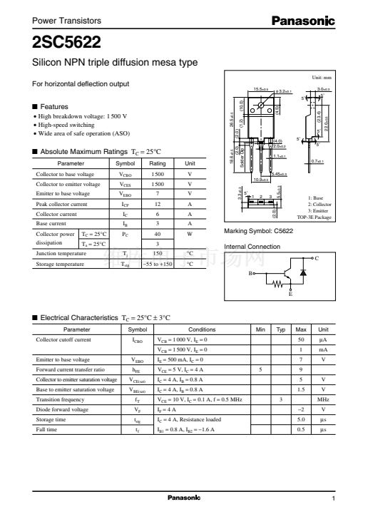
1: Base
2: Collector
3: Emitter
TOP-3E Package
Marking Symbol: C5622
Internal Connection
C
B
Junction temperature
Storage temperature
E
I
Electrical Characteristics
T
C
=
25擄C
鹵
3擄C
Parameter
Collector cutoff current
Symbol
I
CBO
V
EBO
h
FE
V
CE(sat)
V
BE(sat)
f
T
V
F
t
stg
t
f
Conditions
V
CB
=
1 000 V, I
E
=
0
V
CB
=
1 500 V, I
E
=
0
Emitter to base voltage
Forward current transfer ratio
Collector to emitter saturation voltage
Base to emitter saturation voltage
Transition frequency
Diode forward voltage
Storage time
Fall time
I
E
=
500 mA, I
C
=
0
V
CE
=
5 V, I
C
=
4 A
I
C
=
4 A, I
B
=
0.8 A
I
C
=
4 A, I
B
=
0.8 A
V
CE
=
10 V, I
C
=
0.1 A, f
=
0.5 MHz
I
F
=
4 A
I
C
=
4 A, Resistance loaded
I
B1
=
0.8 A, I
B2
= 鈭?.6
A
3
鈭?
5.0
0.5
5
Min
Typ
Max
50
1
7
9
5
1.5
V
V
MHz
V
碌s
碌s
Unit
碌A(chǔ)
mA
V
22.0
鹵0.5
(1.2)
1


 1
1
