鈥?/div>
���������� ������omponents
21201 Itasca Street Chatsworth
��������
���� ������ �!��"#���
$%�� � � ���� �!��"#���
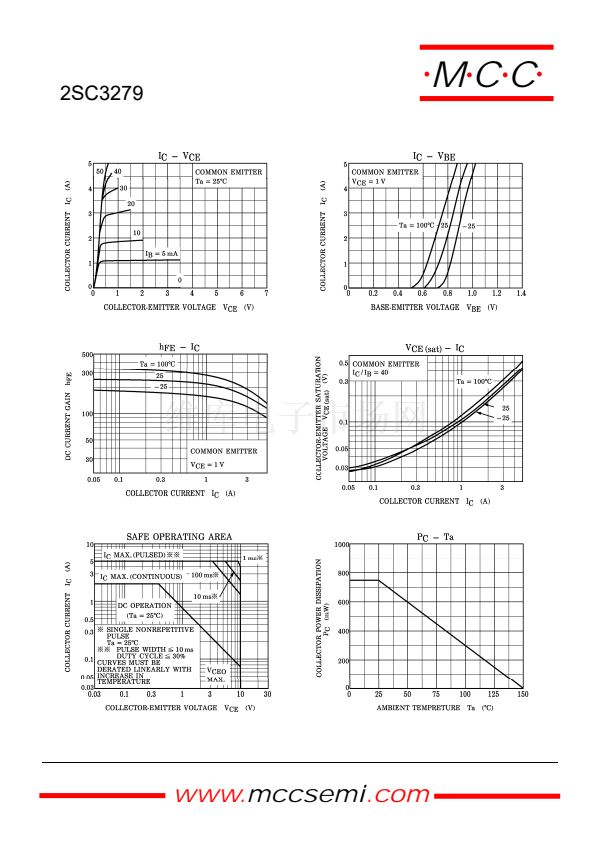
2SC3279
High DC Current Gain and excellent h
FE
Linearity
h
FE(1)
=140-600 (V
CE
=1.0V, I
C
=0.5A)
h
FE(2)
=70 (Min.), 200 (Typ.) (V
CE
=1.0V, I
C
=2.0A)
NPN Silicon
Epitaxial Transistors
TO-92
A
E
Pin Configuration
Bottom View
E
C
B
Maximum Ratings
Symbol
V
CEO
V
CES
V
CBO
V
EBO
I
C
I
B
P
C
T
J
T
STG
Symbol
Rating
Collector-Emitter Voltage
Collector-Emitter Voltage
Collector-Base Voltage
Emitter-Base Voltage
Collector Current - DC
Pulsed
(1)
Base Current
Collector power dissipation
Junction Temperature
Storage Temperature
Parameter
Collector-Emitter Voltage
(I
C
=10mAdc, I
B
=0)
Collector-Emitter Voltage
(I
E
=1.0mAdc, I
C
=0)
Collector Cutoff Current
(V
CB
=30Vdc,I
E
=0)
Emitter Cutoff Current
(V
EB
=6.0Vdc, I
C
=0)
Min
10
6.0
---
---
Rating
10
30
30
6.0
2.0
5.0
0.2
750
-55 to +150
-55 to +150
Typ
---
---
---
---
Max
---
---
0.1
0.1
Unit
V
V
V
V
A
A
W
O
C
O
C
Units
Vdc
Vdc
uAdc
uAdc
B
C
Electrical Characteristics @ 25
O
C Unless Otherwise Specified
OFF CHARACTERISTICS
V
(BR)CEO
V
(BR)EBO
I
CBO
I
EBO
D
ON CHARACTERISTICS
DC Current Gain
(2)
(I
C
=0.5Adc, V
CE
=1.0Vdc)
140
---
600
h
FE(2)
DC Current Gain
(I
C
=2.0Adc, V
CE
=1.0Vdc)
70
200
---
V
CE(sat)
Collector Saturation Voltage
(I
C
=2.0Adc, I
B
=50mAdc)
---
0.2
0.5
V
BE
Base Saturation Voltage
(I
C
=2.0Adc, V
CE
=1.0Vdc)
---
0.86
1.5
f
T
Transition Frequency
(V
CE
=1.0Vdc, I
C
=0.5Adc)
---
150
---
C
ob
Collector Output Capacitance
(V
CB
=10Vdc, I
E
=0, f=1.0MHz)
---
27
---
(1) Pulse Width=10 ms (Max.), Duty Cycle=30% (Max.)
(2) h
FE(1)
Classification L: 140-240, M: 200-330, N: 300-450, P: 420-600
h
FE(1)
---
G
DIMENSIONS
---
Vdc
Vdc
MHz
pF
DIM
A
B
C
D
E
G
INCHES
MIN
.175
.175
.500
.016
.135
.095
MAX
.185
.185
---
.020
.145
.105
MM
MIN
4.45
4.46
12.7
0.41
3.43
2.42
MAX
4.70
4.70
---
0.63
3.68
2.67
NOTE
www.mccsemi.com


 1
1
 2
2
