Transistor
2SB779
Silicon PNP epitaxial planer type
For low-frequency output amplification
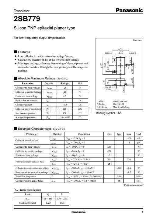
Unit: mm
s
Features
q
q
q
2.8
鈥?.3
0.65鹵0.15
+0.2
+0.25
1.5
鈥?.05
0.65鹵0.15
2
+0.2
1.1
鈥?.1
Parameter
Collector to base voltage
Collector to emitter voltage
Emitter to base voltage
Peak collector current
Collector current
Collector power dissipation
Junction temperature
Storage temperature
Symbol
V
CBO
V
CEO
V
EBO
I
CP
I
C
P
C
T
j
T
stg
Ratings
鈥?5
鈥?0
鈥?
鈥?
鈥?0.5
200
150
鈥?5 ~ +150
Unit
V
V
V
A
A
mW
藲C
藲C
1:Base
2:Emitter
3:Collector
JEDEC:TO鈥?36
EIAJ:SC鈥?9
Mini Type Package
Marking symbol
: 1A
s
Electrical Characteristics
Parameter
Collector cutoff current
Collector to base voltage
Collector to emitter voltage
Emitter to base voltage
Forward current transfer ratio
Collector to emitter saturation voltage
Base to emitter saturation voltage
Transition frequency
Collector output capacitance
(Ta=25藲C)
Symbol
I
CBO
I
CEO
V
CBO
V
CEO
V
EBO
h
FE1*1
h
FE2
V
CE(sat)
V
BE(sat)
f
T
C
ob
Conditions
V
CB
= 鈥?5V, I
E
= 0
V
CE
= 鈥?0V, I
B
= 0
I
C
= 鈥?0碌A(chǔ), I
E
= 0
I
C
= 鈥?mA, I
B
= 0
I
E
= 鈥?0碌A(chǔ), I
C
= 0
V
CE
= 鈥?V, I
C
= 鈥?.5A
*2
V
CE
= 鈥?V, I
C
= 鈥?A
*2
I
C
= 鈥?00mA, I
B
= 鈥?0mA
*2
I
C
= 鈥?00mA, I
B
= 鈥?0mA
*2
V
CB
= 鈥?0V, I
E
= 50mA, f = 200MHz
V
CB
= 鈥?0V, I
E
= 0, f = 1MHz
150
15
*2
min
typ
0 to 0.1
0.1 to 0.3
0.4鹵0.2
0.8
max
鈥?00
鈥?
0.16
鈥?.06
s
Absolute Maximum Ratings
+0.1
(Ta=25藲C)
0.4
鈥?.05
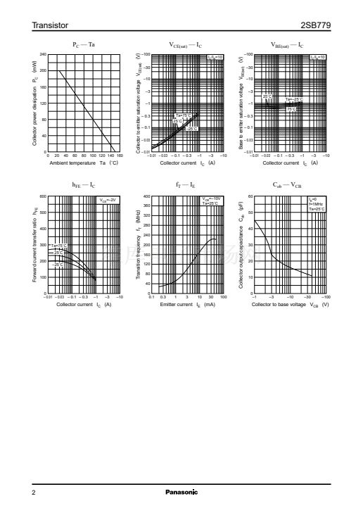
Low collector to emitter saturation voltage V
CE(sat)
.
Satisfactory linearity of h
FE
at the low collector voltage.
Mini type package, allowing downsizing of the equipment and
automatic insertion through the tape packing and the magazine
packing.
0.95
2.9
鈥?.05
1
1.9鹵0.2
+0.2
0.95
3
+0.1
1.45
Unit
nA
碌A(chǔ)
V
V
V
鈥?5
鈥?0
鈥?
90
25
鈥?0.2
鈥?0.4
鈥?.2
220
V
V
MHz
pF
Pulse measurement
*
h
FE1
Rank classification
Rank
h
FE1
Q
90 ~ 155
1AQ
R
130 ~ 220
1AR
Marking Symbol
1


 1
1
 2
2
