鈥?/div>
Equivalent NPN transistor is the 2SC3583.
_
2.9+0.2
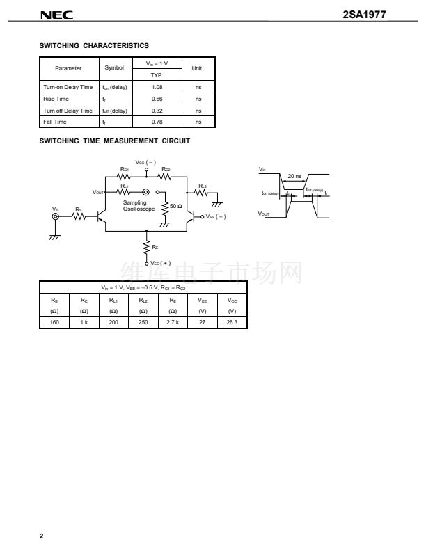
High-speed switching characterstics
2
0.95
Parameter
Collector to Base Voltage
Collector to Emitter Voltage
Emitter to Base Voltage
Collector Current
Total Power Dissipation
Junction Temperature
Storage Temperature
Symbol
V
CB0
V
CE0
V
EB0
I
C
P
T
T
j
T
stg
Rating
鈭?0
鈭?2
鈭?.0
鈭?0
200
150
鈭?5
to +150
Unit
V
V
V
mA
mW
擄C
擄C
1.1 to 1.4
0.3
Marking
0.16
+0.1
鈥?.06
ELECTRICAL CHARACTERISTICS (T
A
= 25
擄
C)
Parameter
Collector Cutoff Current
Emitter Cutoff Current
DC Current Gain
Gain Bandwidth Product
Collector Capacitance
Insertion Power Gain
Noise Figure
Symbol
I
CB0
I
EB0
h
FE
f
T
C
re
*
| S
21e
|
NF
2
PIN CONNECTIONS
1: Emitter
2: Base
3: Collector Marking; T92
Test Conditions
V
CB
=
鈭?0
V
V
EB
=
鈭?
V
V
CE
=
鈭?
V, I
C
=
鈭?0
mA
V
CE
=
鈭?
V, I
C
=
鈭?0
mA, f = 1 GHz
V
CB
=
鈭?0
V, I
E
= 0, f = 1 MHz
V
CE
=
鈭?
V, I
C
=
鈭?0
mA, f = 1.0 GHz
V
CE
=
鈭?
V, I
C
=
鈭?
mA, f = 1 GHz
MIN.
TYP.
0 to 0.1
MAX.
鈭?.1
鈭?.1
0.4
+0.1
鈥?.05
ABSOLUTE MAXIMUM RATINGS (T
A
= 25
擄
C)
1
3
Unit
碌
A
碌
A
20
6.0
8.5
0.5
8.0
12.0
1.5
100
GHz
1
pF
dB
3
dB
* Mesured by a 3-terminal bridge. Emitter and Case should be connected to the guard terminal.
h
FE
Classification
Rank
Marking
h
FE
FB
T92
20 to 100
Document No. P10925EJ1V0DS00 (1st edition)
Date Published April 1996 P
Printed in Japan
漏
1996


 1
1
 2
2
 3
3
 4
4
 5
5
 6
6
 7
7
 8
8
 9
9
 10
10
 11
11
 12
12
