Transistor
2SA1961
Silicon PNP epitaxial planer type
For general amplification
Complementary to 2SC5419
6.9鹵0.1
0.15
Unit: mm
1.05 2.5鹵0.1
鹵0.05
(1.45)
0.8
0.5
4.5鹵0.1
0.45
鈥?.05
2.5鹵0.1
0.7
4.0
s
Features
q
0.65 max.
1.0 1.0
0.2
High collector to emitter voltage V
CEO
.
s
Absolute Maximum Ratings
Parameter
Collector to base voltage
Collector to emitter voltage
Emitter to base voltage
Peak collector current
Collector current
Collector power dissipation
Junction temperature
Storage temperature
*
(Ta=25藲C)
Ratings
鈥?00
鈥?00
鈥?
鈥?0.1
鈥?0
Unit
V
V
V
A
mA
W
藲C
藲C
Note: In addition to the
lead type shown in
the upper figure, the
type as shown in
the lower figure is
also available.
0.45
鈥?.05
+0.1
+0.1
Symbol
V
CBO
V
CEO
V
EBO
I
CP
I
C
P
C
T
j
T
stg
*
2.5鹵0.5
1
2
2.5鹵0.5
3
1
150
鈥?5 ~ +150
1:Emitter
2:Collector
3:Base
MT2 Type Package
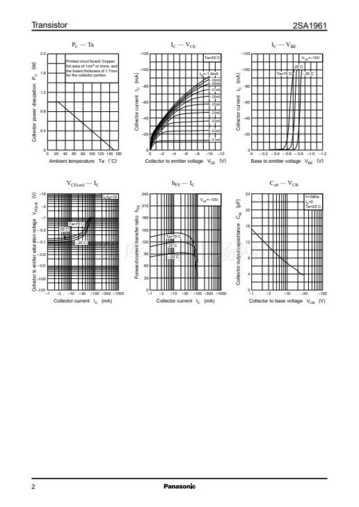
Printed circuit board: Copper foil area of 1cm
2
or more, and the board
thickness of 1.7mm for the collector portion
1.2鹵0.1
0.65
max.
0.45
+0.1
鈥?0.05
(HW type)
s
Electrical Characteristics
Parameter
Collector to emitter voltage
Emitter to base voltage
Forward current transfer ratio
Collector to emitter saturation voltage
Transition frequency
Collector output capacitance
(Ta=25藲C)
Symbol
V
CEO
V
EBO
h
FE*1
V
CE(sat)
f
T
C
ob
Conditions
I
C
= 鈥?00碌A(chǔ), I
B
= 0
I
E
= 鈥?碌A(chǔ), I
C
= 0
V
CE
= 鈥?0V, I
C
= 鈥?mA
I
C
= 鈥?0mA, I
B
= 鈥?mA
V
CB
= 鈥?V, I
E
= 10mA, f = 200MHz
V
CB
= 鈥?0V, I
E
= 0, f = 1MHz
30
7
min
鈥?00
鈥?
30
150
鈥?.5
typ
max
Unit
V
V
鈥?/div>
V
MHz
pF
*1
h
FE
Rank classification
P
30 ~ 100
Q
60 ~ 150
Rank
h
FE
14.5鹵0.5
1


 1
1
 2
2
 3
3
