鈮?/div>
30碌m at 80% BVDSS
鈥?Gamma Dot
鈥?Photo Current
鈥?Neutron
鈥?Single Event
Description
The Harris Semiconductor Sector has designed a series of SECOND GENERA-
TION hardened power MOSFETs of both N and P channel enhancement types
with ratings from 100V to 500V, 1A to 60A, and on resistance as low as 25m鈩?
Total dose hardness is offered at 100K RAD(Si) and 1000KRAD(Si) with neutron
hardness ranging from 1E13n/cm
2
for 500V product to 1E14n/cm
2
for 100V prod-
uct. Dose rate hardness (GAMMA DOT) exists for rates to 1E9 without current lim-
iting and 2E12 with current limiting. Heavy ion survival from signal event drain
burn-out exists for linear energy transfer (LET) of 35 at 80% of rated voltage.
This MOSFET is an enhancement-mode silicon-gate power 鏗乪ld effect transistor of
the vertical DMOS (VDMOS) structure. It is specially designed and processed to
exhibit minimal characteristic changes to total dose (GAMMA) and neutron (n
o
)
exposures. Design and processing efforts are also directed to enhance survival to
heavy ion (SEE) and/or dose rate (GAMMA DOT) exposure.
This part may be supplied as a die or in various packages other than shown above.
Reliability screening is available as either non TX (commercial), TX equivalent of
MIL-S-19500, TXV equivalent of MIL-S-19500, or space equivalent of MIL-S-
19500. Contact the Harris Semiconductor High-Reliability Marketing group for any
desired deviations from the data sheet.
Symbol
Absolute Maximum Ratings
(TC = +25
o
C) Unless Otherwise Speci鏗乪d
2N7288D, R, H
250
250
9
6
27
鹵20
75
30
0.60
27
9
27
-55 to +150
300
UNITS
V
V
A
A
A
V
W
W
W/
o
C
A
A
A
o
C
o
C
Drain-Source Voltage. . . . . . . . . . . . . . . . . . . . . . . . . . . . . . . . . . . . . . . . . . . . . . . . . . . . . . .VDS
Drain-Gate Voltage (RGS = 20k鈩? . . . . . . . . . . . . . . . . . . . . . . . . . . . . . . . . . . . . . . . . . . VDGR
Continuous Drain Current
TC = +25
o
C . . . . . . . . . . . . . . . . . . . . . . . . . . . . . . . . . . . . . . . . . . . . . . . . . . . . . . . . . . . . . .ID
TC = +100
o
C . . . . . . . . . . . . . . . . . . . . . . . . . . . . . . . . . . . . . . . . . . . . . . . . . . . . . . . . . . . . .ID
Pulsed Drain Current . . . . . . . . . . . . . . . . . . . . . . . . . . . . . . . . . . . . . . . . . . . . . . . . . . . . . . . IDM
Gate-Source Voltage . . . . . . . . . . . . . . . . . . . . . . . . . . . . . . . . . . . . . . . . . . . . . . . . . . . . . . .VGS
Maximum Power Dissipation
TC = +25
o
C . . . . . . . . . . . . . . . . . . . . . . . . . . . . . . . . . . . . . . . . . . . . . . . . . . . . . . . . . . . . . PT
TC = +100
o
C . . . . . . . . . . . . . . . . . . . . . . . . . . . . . . . . . . . . . . . . . . . . . . . . . . . . . . . . . . . . PT
Derated Above +25
o
C . . . . . . . . . . . . . . . . . . . . . . . . . . . . . . . . . . . . . . . . . . . . . . . . . . . . . . .
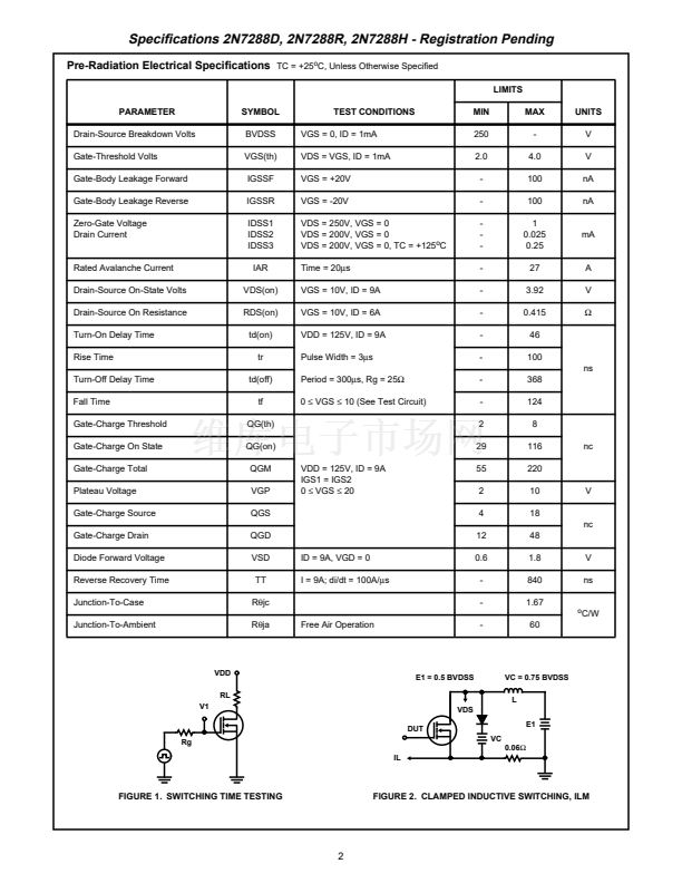
Inductive Current, Clamped, L = 100碌H, (See Test Figure). . . . . . . . . . . . . . . . . . . . . . . . . . ILM
Continuous Source Current (Body Diode) . . . . . . . . . . . . . . . . . . . . . . . . . . . . . . . . . . . . . . . . . IS
Pulsed Source Current (Body Diode) . . . . . . . . . . . . . . . . . . . . . . . . . . . . . . . . . . . . . . . . . . ISM
Operating And Storage Temperature. . . . . . . . . . . . . . . . . . . . . . . . . . . . . . . . . . . . . TJC, TSTG
Lead Temperature (During Soldering)
Distance > 0.063 in. (1.6mm) From Case, 10s Max. . . . . . . . . . . . . . . . . . . . . . . . . . . . . . . TL
CAUTION: These devices are sensitive to electrostatic discharge. Users should follow proper I.C. Handling Procedures.
Copyright
漏
Harris Corporation 1992
File Number
3256.1
1


 1
1
 2
2
 3
3
 4
4
 5
5
