鈮?/div>
1.0
碌s,
T
C
= 90擄C)
Operating Junction Temperature Range
Storage Temperature Range
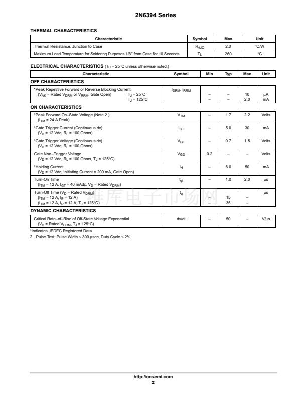
*Indicates JEDEC Registered Data
1. V
DRM
and V
RRM
for all types can be applied on a continuous basis. Ratings
apply for zero or negative gate voltage; however, positive gate voltage shall
not be applied concurrent with negative potential on the anode. Blocking
voltages shall not be tested with a constant current source such that the
voltage ratings of the devices are exceeded.
Symbol
V
DRM,
V
RRM
50
100
400
800
I
T(RMS)
I
TSM
I
2
t
P
GM
P
G(AV)
I
GM
T
J
T
stg
12
100
40
20
0.5
2.0
鈥?0 to
+125
鈥?0 to
+150
A
A
A
2
s
Watts
Watts
A
擄C
擄C
1
2
3
4
1
2
3
x
= 4, 5, 7 or 9
YY = Year
WW = Work Week
Value
Unit
Volts
http://onsemi.com
SCRs
12 AMPERES RMS
50 thru 800 VOLTS
G
A
K
MARKING
DIAGRAM
4
TO鈥?20AB
CASE 221A
STYLE 3
YY WW
639x
PIN ASSIGNMENT
Cathode
Anode
Gate
Anode
ORDERING INFORMATION
Device
2N6394
2N6395
2N6397
2N6399
Package
TO220AB
TO220AB
TO220AB
TO220AB
Shipping
500/Box
500/Box
500/Box
500/Box
Preferred
devices are recommended choices for future use
and best overall value.
漏
Semiconductor Components Industries, LLC, 2001
1
April, 2001 鈥?Rev. 3
Publication Order Number:
2N6394/D


 1
1
 2
2
 3
3
 4
4
 5
5
 6
6
 7
7
 8
8
