2N5564/5565/5566
Vishay Siliconix
Matched N-Channel JFET Pairs
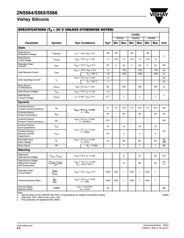
PRODUCT SUMMARY
Part Number
2N5564
2N5565
2N5566
V
GS(off)
(V)
鈥?.5 to 鈥?
鈥?.5 to 鈥?
鈥?.5 to 鈥?
V
(BR)GSS
Min (V)
鈥?0
鈥?0
鈥?0
g
fs
Min (mS)
7.5
7.5
7.5
I
G
Typ (pA)
鈥?
鈥?
鈥?
jV
GS1
鈥?V
GS2
j
Max (mV)
5
10
20
FEATURES
D
D
D
D
D
D
D
Two-Chip Design
High Slew Rate
Low Offset/Drift Voltage
Low Gate Leakage: 3 pA
Low Noise: 12
nV鈦勨垰Hz
@ 10 Hz
Good CMRR: 76 dB
Minimum Parasitics
BENEFITS
D
Tight Differential Match vs. Current
D
Improved Op Amp Speed, Settling Time
Accuracy
D
Minimum Input Error/Trimming Requirement
D
Insignificant Signal Loss/Error Voltage
D
High System Sensitivity
D
Minimum Error with Large Input Signals
D
Maximum High Frequency Performance
APPLICATIONS
D
Wideband Differential Amps
D
High-Speed,
Temp-Compensated,
Single-Ended Input Amps
D
High-Speed Comparators
D
Impedance Converters
D
Matched Switches
DESCRIPTION
The 2N5564/5565/5566 are matched pairs of JFETs mounted
in a TO-71 package. This two-chip design reduces parasitics
for good performance at high frequency while ensuring
extremely tight matching.
This series features high
breakdown voltage (V
(BR)DSS
typically > 55 V), high gain
(typically > 9 mS), and <5 mV offset between the two die.
The hermetically-sealed TO-71 package is available with full
military processing (see Military Information).
For similar products see the low-noise U/SST401 series, and
the low-leakage 2N5196/5197/5198/5199 data sheets.
TO-71
S
1
1
D
1
6
D
2
G
2
2
5
3
G
1
Top View
4
S
2
ABSOLUTE MAXIMUM RATINGS
Gate-Drain, Gate-Source Voltage . . . . . . . . . . . . . . . . . . . . . . . . . . . . . . . 鈥?0 V
Gate-Gate Voltage . . . . . . . . . . . . . . . . . . . . . . . . . . . . . . . . . . . . . . . . . . . .
"80
V
Gate Current . . . . . . . . . . . . . . . . . . . . . . . . . . . . . . . . . . . . . . . . . . . . . . . . . 50 mA
Lead Temperature (
1
/
16
鈥?from case for 10 sec.) . . . . . . . . . . . . . . . . . . 300
_C
Storage Temperature . . . . . . . . . . . . . . . . . . . . . . . . . . . . . . . . . . . 鈥?5 to 200_C
Document Number: 70254
S-04031鈥擱ev. D, 04-Jun-01
Operating Junction Temperature . . . . . . . . . . . . . . . . . . . . . . . . . . 鈥?5 to 150_C
Power Dissipation :
Per Side
a
. . . . . . . . . . . . . . . . . . . . . . . . 325 mW
Total
b
. . . . . . . . . . . . . . . . . . . . . . . . . . . 650 mW
Notes
a. Derate 2.6 mW/_C above 25_C
b. Derate 5.2 mW/_C above 25_C
www.vishay.com
8-1


 1
1
 2
2
 3
3
 4
4
 5
5
