28C16A
16K (2K x 8) CMOS EEPROM
FEATURES
鈥?Fast Read Access Time鈥?50 ns
鈥?CMOS Technology for Low Power Dissipation
- 30 mA Active
- 100
碌
A Standby
鈥?Fast Byte Write Time鈥?00
碌
s or 1 ms
鈥?Data Retention >200 years
鈥?High Endurance - Minimum 10
4
Erase/Write Cycles
鈥?Automatic Write Operation
- Internal Control Timer
- Auto-Clear Before Write Operation
- On-Chip Address and Data Latches
鈥?Data polling
鈥?Chip Clear Operation
鈥?Enhanced Data Protection
- V
CC
Detector
- Pulse Filter
- Write Inhibit
鈥?Electronic Signature for Device Identi鏗乧ation
鈥?5-Volt-Only Operation
鈥?Organized 2Kx8 JEDEC Standard Pinout
鈥?24-pin Dual-In-Line Package
鈥?32-pin PLCC Package
鈥?28-pin Thin Small Outline Package (TSOP)
8x20mm
鈥?28-pin Very Small Outline Package (VSOP)
8x13.4mm
鈥?Available for Extended Temperature Ranges:
- Commercial: 0藲C to +70藲C
- Industrial: -40藲C to +85藲C
PACKAGE TYPES
32
Vcc
31
WE
18
19
4
A7
3
NC
2
NC
1
NU
鈥?Pin 1 indicator on PLCC on top of package
OE
NC
A9
A8
NC
WE
Vcc
NC
NC
A7
A6
A5
A4
A3
1
2
3
4
5
6
7
8
9
10
11
12
13
14
OE
NC
A9
A8
NC
WE
V
CC
NC
NC
A7
A6
A5
A4
A3
22
23
24
25
26
27
28
1
2
3
4
5
6
7
I/O1
I/O2
Vss
NU
I/O3
I/O4
I/O5
28
27
26
25
24
23
22
21
20
19
18
17
16
15
21
20
19
18
17
16
15
14
13
12
11
10
9
8
A10
CE
I/O7
I/O6
I/O5
I/O4
I/O3
V
SS
I/O2
I/O1
I/O0
A0
A1
A2
A7
A6
A5
A4
A3
A2
A1
A0
I/O0
I/O1
I/O2
V
SS
鈥?
2
3
4
5
6
7
8
9
10
11
12
24
23
22
21
20
19
18
17
16
15
14
13
Vcc
A8
A6
A9
A5
WE
A4
OE
A3
A10
A2
CE
A1
I/O7 A0
I/O6 NC
I/O5 I/O0
I/O4
I/O3
30
NC
29
A8
28
A9
27
NC
26
NC
25
OE
24
A10
23
CE
22
I/O7
21
I/O6
20
5
6
7
PLCC
8
9
10
11
12
13
14
15
16
17
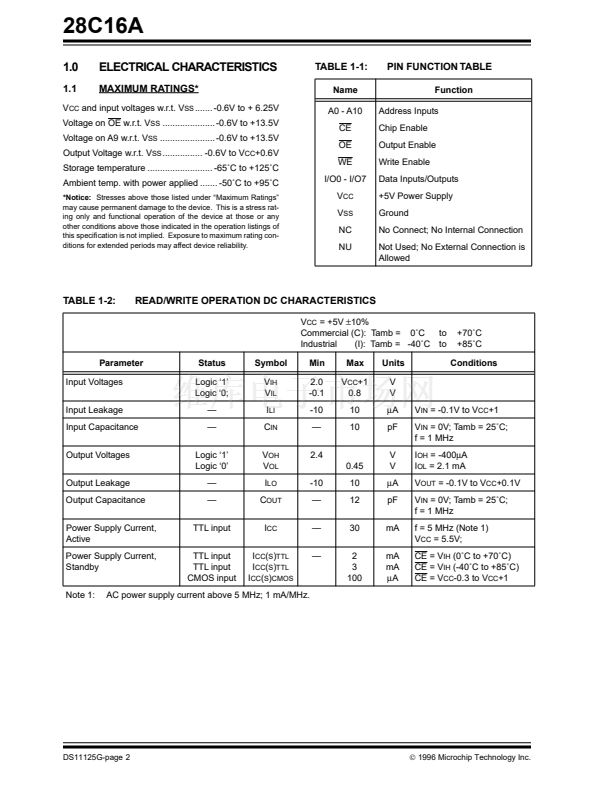
DESCRIPTION
The Microchip Technology Inc. 28C16A is a CMOS 16K
non-volatile electrically Erasable PROM. The 28C16A
is accessed like a static RAM for the read or write
cycles without the need of external components. Dur-
ing a 鈥渂yte write鈥? the address and data are latched
internally, freeing the microprocessor address and data
bus for other operations. Following the initiation of
write cycle, the device will go to a busy state and auto-
matically clear and write the latched data using an
internal control timer. To determine when a write cycle
is complete, the 28C16A uses Data polling. Data poll-
ing allows the user to read the location last written to
when the write operation is complete. CMOS design
and processing enables this part to be used in systems
where reduced power consumption and reliability are
required. A complete family of packages is offered to
provide the utmost 鏗俥xibility in applications.
BLOCK DIAGRAM
I/O0
I/O7
DIP
A10
CE
I/07
I/06
I/05
I/04
I/03
Vss
I/02
I/01
I/00
A0
A1
A2
TSOP
VSOP
V
SS
V
CC
CE
OE
WE
Data Protection
Circuitry
Chip Enable/
Output Enable
Control Logic
Auto Erase/Write
Timing
Data
Poll
Input/Output
Buffers
Program Voltage
Generation
A0
L
a
t
c
h
e
s
A10
Y
Decoder
Y Gating
X
Decoder
16K bit
Cell Matrix
漏
1996 Microchip Technology Inc.
DS11125G-page 1
This document was created with FrameMaker 4 0 4


 1
1
 2
2
 3
3
 4
4
 5
5
 6
6
 7
7
 8
8
