FINAL
Am27C2048
2 Megabit (128 K x 16-Bit) CMOS EPROM
DISTINCTIVE CHARACTERISTICS
s
Fast access time
鈥?Speed options as fast as 55 ns
s
Low power consumption
鈥?100 碌A maximum CMOS standby current
s
JEDEC-approved pinout
鈥?Plug-in upgrade of 1 Mbit EPROM
鈥?40-pin DIP/PDIP
鈥?44-pin PLCC
s
Single +5 V power supply
s
鹵10%
power supply tolerance standard
s
100% Flashrite programming
鈥?Typical programming time of 16 seconds
s
Latch-up protected to 100 mA from 鈥? V to
V
CC
+ 1 V
s
Versatile features for simple interfacing
鈥?Both CMOS and TTL input/output compatibility
鈥?Two line control functions
s
High noise immunity
GENERAL DESCRIPTION
The Am27C2048 is a 2 Mbit, ultraviolet erasable pro-
grammable read-only memory. It is organized as 128 K
words, operates from a single +5 V supply, has a static
standby mode, and features fast single address loca-
tion programming. The Am27C2048 is ideal for use in
16-bit microprocessor systems. The device is available
in windowed ceramic DIP packages, and plastic one
time programmable (OTP) PDIP and PLCC packages.
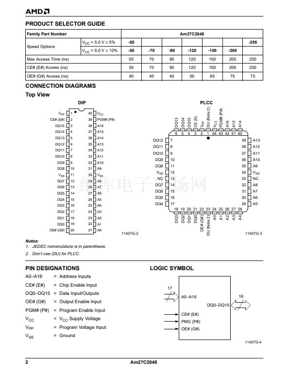
Data can be typically accessed in less than 55 ns, al-
lowing high-performance microprocessors to operate
without any WAIT states. The device offers separate
Output Enable (OE#) and Chip Enable (CE#) controls,
thus eliminating bus contention in a multiple bus micro-
processor system.
AMD鈥檚 CMOS process technology provides high
speed, low power, and high noise immunity. Typical
power consumption is only 125 mW in active mode,
and 100 碌W in standby mode.
All signals are TTL levels, including programming sig-
nals. Bit locations may be programmed singly, in
blocks, or at random. The device supports AMD鈥檚
Flashrite programming algorithm (100 碌s pulses), re-
sulting in a typical programming time of 16 seconds.
BLOCK DIAGRAM
V
CC
V
SS
V
PP
OE#
CE#
PGM#
Output Enable
Chip Enable
and
Prog Logic
Y
Decoder
A0鈥揂16
Address
Inputs
Output
Buffers
Data Outputs
DQ0鈥揇Q15
Y
Gating
X
Decoder
2,097,152
Bit Cell
Matrix
11407G-1
Publication#
11407
Rev:
G
Amendment/0
Issue Date:
May 1998


 1
1
 2
2
 3
3
 4
4
 5
5
 6
6
 7
7
 8
8
 9
9
 10
10
 11
11
 12
12
