Design Considerations for the Am79761 Gigabit
Ethernet Physical Layer GigaPHY鈩?SD Device
Application Note
This document is intended to assist customers in using AMD鈥檚 Gigabit Ethernet Physical Layer
devices. Details concerning application information, circuit design, PCB layout, and component se-
lection are provided to help ensure 鏗乺st-pass success in implementing a functional design which has
optimized signal quality.
INTRODUCTION
This document is applicable to the Am79761
GigaPHY-SD product. This document should be used
in conjunction with the product data sheet. An elemen-
tary knowledge of Ethernet and high speed printed cir-
cuit layout techniques is assumed. Contact your local
AMD Field Applications Engineer or Sales Of鏗乧e to dis-
cuss any questions and concerns you may have.
are present at all inputs (GigaPHY-SD and Encoder/
Decoder), and that the proper phase relationship is
maintained between the GigaPHY-SD device and En-
coder/Decoder chip, since the GigaPHY-SD device
latches data on the rising edge of this clock. The Giga-
PHY-SD device provides a TTL input buffer which does
not support AC-coupling of the REFCLK signal.
Although oscillators provide the cleanest source for
REFCLK, oscillators over 100 MHz often cost more
than may be acceptable for a speci鏗乧 design. In this
case, customers have used clock generator chips to
provide REFCLK at a lower cost than an oscillator. Un-
fortunately, the cost reduction is accompanied by a sig-
ni鏗乧ant increase in REFCLK jitter, which adds jitter to
the transmitted serial data resulting in a reduction in the
maximum transmission distance.
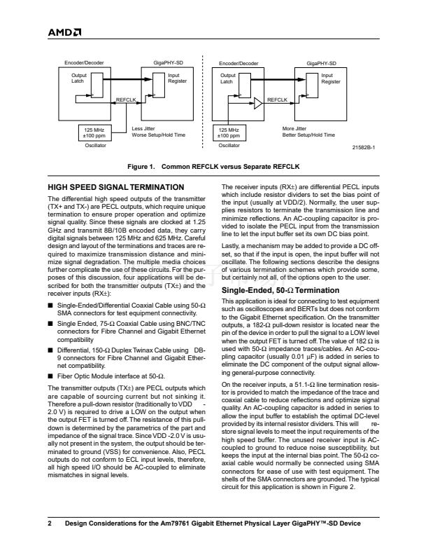
Another con鏗乬uration is to generate the REFCLK in the
Encoder/Decoder chip. This is desirable where the
REFCLK is used to latch incoming transmit data, since
it may be easier to meet the setup/hold time require-
ments of the transmitter, especially when using a 10-bit
interface at 125 MHz. When the oscillator drives
REFCLK and the Encoder/Decoder chip, the clock-to-
output delay of the Encoder/Decoder chip impacts the
setup/hold time of the data bus with respect to the REF-
CLK. When the Encoder/Decoder chip generates REF-
CLK, the output buffer for REFCLK and the output latch
for transmit data track each other and thereby increase
setup time. However, the penalty for this scheme is in-
creased jitter added by the Encoder/Decoder chip to
the REFCLK. The two con鏗乬urations for REFCLK gen-
eration are shown in Figure 1.
Where possible, it is recommended to let the oscillator
drive both the Encoder/Decoder chip and the GigaPHY-
SD device in order to provide the cleanest REFCLK.
CLOCK GENERATION
One of the most important aspects of the design is gen-
eration of the REFCLK signal. This input provides the
reference clock for the internal PLL which is multiplied
by 10x or 20x to generate the baud rate clock.The ris-
ing edge of REFCLK is continuously phase compared
to the internal baud rate clock so that the PLL will
speed up or slow down the VCO in order to keep these
two signals aligned. It is therefore important that the
REFCLK be as jitter-free as possible in order to mini-
mize jitter introduced into the PLL and its baud rate
clock. It is also desirable to have fast rising edges on
this clock to minimize the time in which the signal tran-
sitions from a LOW level to a HIGH level. A fast edge
will reduce edge-detection ambiguity in the input buffer
and therefore reduce jitter in the PLL.
Note:
The rising edge of this clock also latches the data
on the transmit bus into the input latch so care must be
taken to ensure that the transmit data bus meets the
setup and hold time requirements of the transmitter.
The most desirable solution for generating REFCLK is
to have a crystal oscillator drive the input to an En-
coder/Decoder that interfaces to the GigaPHY-SD or
MAC device. In some cases, this oscillator will also
have to drive a clock input to the Encoder/Decoder.
Care must be taken to ensure that good quality signals
This document contains information on a product under development at Advanced Micro Devices. The information
is intended to help you evaluate this product. AMD reserves the right to change or discontinue work on this proposed
product without notice.
Publication#
21582
Rev:
B
Amendment/0
Issue Date:
May 1998
Refer to AMD鈥檚 Website (www.amd.com) for the latest information.


 1
1
 2
2
 3
3
 4
4
 5
5
 6
6
 7
7
 8
8
