鈥?/div>
Working Peak Reverse Voltage Range 鈥?10 V to 78 V
Standard Zener Breakdown Voltage Range 鈥?11.7 V to 91.3 V
Peak Power 鈥?600 Watts @ 1 ms
ESD Rating of Class 3 (> 16 KV) per Human Body Model
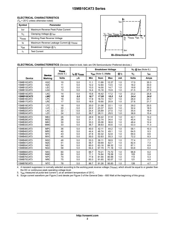
Maximum Clamp Voltage @ Peak Pulse Current
Low Leakage < 5
碌A(chǔ)
Above 10 V
UL 497B for Isolated Loop Circuit Protection
Response Time is Typically < 1 ns
SMB
CASE 403A
PLASTIC
Mechanical Characteristics:
CASE:
Void-free, transfer-molded, thermosetting plastic
FINISH:
All external surfaces are corrosion resistant and leads are
readily solderable
MAXIMUM CASE TEMPERATURE FOR SOLDERING PURPOSES:
MARKING DIAGRAM
YWW
xxC
Y
WW
xxC
= Year
= Work Week
= Specific Device Code
=
(See Table Next Page)
260擄C for 10 Seconds
LEADS:
Modified L鈥揃end providing more contact area to bond pads
POLARITY:
Polarity band will not be indicated
MOUNTING POSITION:
Any
MAXIMUM RATINGS
Rating
Peak Power Dissipation (Note 1.)
@ T
L
= 25擄C, Pulse Width = 1 ms
DC Power Dissipation @ T
L
= 75擄C
Measured Zero Lead Length (Note 2.)
Derate Above 75擄C
Thermal Resistance from Junction to Lead
DC Power Dissipation (Note 3.) @ T
A
= 25擄C
Derate Above 25擄C
Thermal Resistance from Junction
to Ambient
Operating and Storage
Temperature Range
Symbol
P
PK
P
D
Value
600
3.0
40
25
0.55
4.4
226
鈥?5 to
+150
Unit
W
W
mW/擄C
擄C/W
W
mW/擄C
擄C/W
擄C
ORDERING INFORMATION
Device
{
1SMBxxCAT3
Package
SMB
Shipping
2500/Tape & Reel
R
qJL
P
D
R
qJA
T
J
, T
stg
Devices listed in
bold, italic
are ON Semiconductor
Preferred
devices.
Preferred
devices are recommended
choices for future use and best overall value.
鈥燭he 鈥淭3鈥?suffix refers to a 13 inch reel.
1. 10 X 1000
ms,
non鈥搑epetitive
2. 1鈥?square copper pad, FR鈥? board
3. FR鈥? board, using ON Semiconductor minimum recommended footprint, as
shown in 403A case outline dimensions spec.
*Please see 1SMB5.0AT3 to 1SMB170AT3 for Unidirectional devices.
漏
Semiconductor Components Industries, LLC, 2001
1
May, 2001 鈥?Rev. 4
Publication Order Number:
1SMB10CAT3/D


 1
1
 2
2
 3
3
 4
4
 5
5
 6
6
 7
7
 8
8
