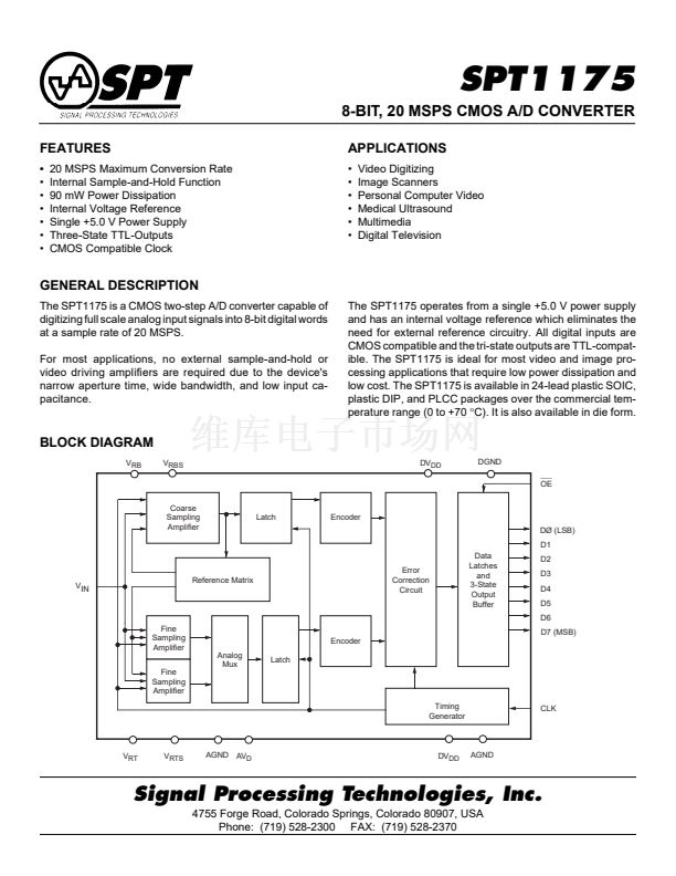
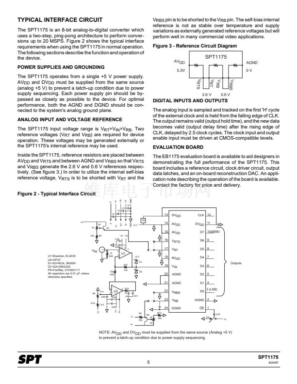
TYPICAL INTERFACE CIRCUIT
The SPT1175 is an 8-bit analog-to-digital converter which
uses a two-step, ping-pong architecture to perform conver-
sions up to 20 MSPS. Figure 2 shows the typical interface
requirements when using the SPT1175 in normal operation.
The following sections describe the function and operation of
the device.
POWER SUPPLIES AND GROUNDING
The SPT1175 operates from a single +5 V power supply.
AV
DD
and DV
DD
must be supplied from the same source
(analog +5 V) to prevent a latch-up condition due to power
supply sequencing. Each power supply pin should be by-
passed as closely as possible to the device. For optimal
performance, both the AGND and DGND should be con-
nected to the system's analog ground plane.
ANALOG INPUT AND VOLTAGE REFERENCE
The SPT1175 input voltage range is V
RT
>V
IN
>V
RB
. Two
reference voltages (V
RT
and V
RB
) are required for device
operation. These voltages may be generated externally or
the SPT1175's internal reference may be used.
Inside the SPT1175, reference resistors are placed between
AV
DD
and V
RTS
and between AGND and V
RBS
so that V
RTS
and V
RBS
generate the 2.6 V and 0.6 V references respec-
tively. (See figure 3.) In order to utilize the internal self-bias
reference voltage, V
RTS
is to be shorted with V
RT
and the
Figure 2 - Typical Interface Circuit
10
10
10 +
10 +
+
+5
R1
2k
Q1
FB
+5 V
GND
-5
+5
+15
-15
+
GND
+15
-5
-15
+5
V
RBS
pin is to be shorted to the V
RB
pin. The self-bias internal
reference is not as stable over temperature and supply
variations as externally generated reference voltages but will
perform well in many commercial video applications.
Figure 3 - Reference Circuit Diagram
SPT1175
AVDD
5.0V
AGND
0V
DIGITAL INPUTS AND OUTPUTS
The analog input is sampled and tracked on the first 'H' cycle
of the external clock and is held from the falling edge of CLK.
The output remains valid (output hold time), and the new data
becomes valid (output delay time) after the rising edge of
CLK, delayed by 2.5 clock cycles. The clock input and output
enable input must be driven at CMOS-compatible levels.
EVALUATION BOARD
The EB1175 evaluation board is available to aid designers in
demonstrating the full performance of the SPT1175. This
board includes a reference circuit, clock driver circuit, output
data latches, and an on-board reconstruction DAC. An appli-
cation note describing the operation of the board is available.
Contact the factory for price and delivery.
VRTS
2.6 V
VRB
VRT
0.6 V
VRBS
13
14
15
DVDD
AVDD
AVDD
VRTS
VRT
AVDD
VIN
AGND
AGND
VRBS
VRB
DGND
CLK 12
DVDD 11
D7 10(MSB)
D6 9
D5 8
D4 7
D3 6
D2 5
D1 4
D0
DGND
3 (LSB)
2
Outputs
750
R9
C28
-15 +15
16
+
4
7
+5 V
D1
R37
C29
VIN
U1=Eleantec, EL2030
U2=OP.07
D1=D2=RCA, SK9091
Q1=Q2=2N2222A
FR=FairRite, 2743001111
All capacitors are 0.01 碌F unless
otherwise specified.
17
18
19
D2
3
75
R35
2 _
U1
750
R36
750
20
21
_
10 k
R6
C58
R10
2
U2
3 +
C59
6 R15
10
C8
C61
22
23
24
R8
-5
750
+5
R2
R13
Q2
2k
200
7.5 k
-15
C60
-15
+15
OE 1
3-ST
EN
+5
NOTE: AVDD and DVDD must be supplied from the same source (Analog +5 V)
to prevent a latch-up condition due to power supply sequencing.
SPT
SPT1175
5
6/24/97


 1
1
 2
2
 3
3
 4
4
 5
5
 6
6
 7
7
 8
8
