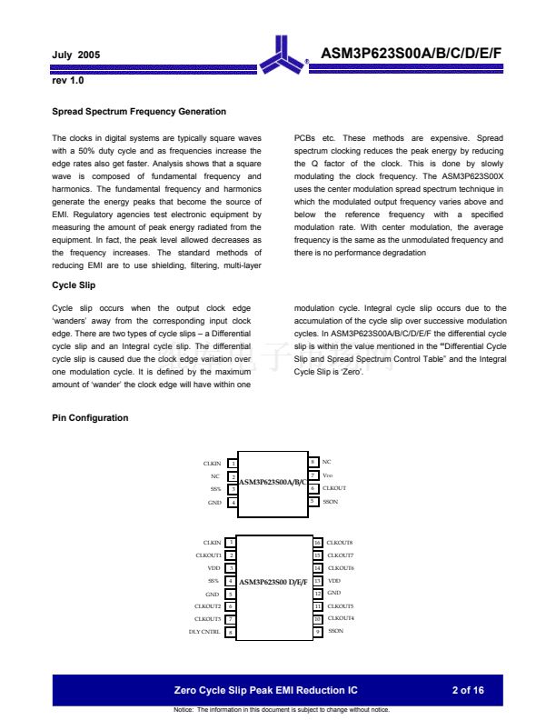
鈩?/div>
V
IN
= VDD
I
OL
= 8mA
I
OH
= -8mA
Unloaded outputs
2.4
15
23
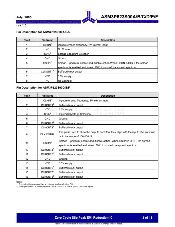
Switching Characteristics for ASM3P623S00A/B/C and ASM3P623S00D/E/F
7
Parameter
1/t
1
t
3
t
4
t
5
t
6
t
7
t
J
t
LOCK
Notes:
5. CLKIN input has a threshold voltage of VDD/2
6. Parameter is guaranteed by design and characterization. Not 100% tested in production
7. All parameters specified with loaded outputs.
Description
Output Frequency
Duty Cycle
6
= (t
2
/ t
1
) * 100
Output Rise Time
6
Output Fall Time
6
Output-to-output skew
6
Delay, CLKIN Rising Edge to
CLKOUT Rising Edge
6
Test Conditions
30pF load
Measured at VDD/2
Measured between 0.8V and 2.0V
Measured between 2.0V and 0.8V
All outputs equally loaded
Measured at VDD /2
Measured at VDD/2 on the CLKOUT pins
of the device
Loaded outputs
Stable power supply, valid clock presented
on CLKIN pin
Min
20
40
Typ
50
Max
50
60
2.5
2.5
250
鹵350
700
200
1.0
Unit
MHz
%
nS
nS
pS
pS
pS
pS
mS
Device-to-Device Skew
6
Cycle-to-cycle jitter
6
PLL Lock Time
6
Zero Cycle Slip Peak EMI Reduction IC
Notice: The information in this document is subject to change without notice.
5 of 16


 1
1
 2
2
 3
3
 4
4
 5
5
 6
6
 7
7
 8
8
 9
9
 10
10
 11
11
 12
12
 13
13
 14
14
 15
15
 16
16
