July 2005
rev 1.0
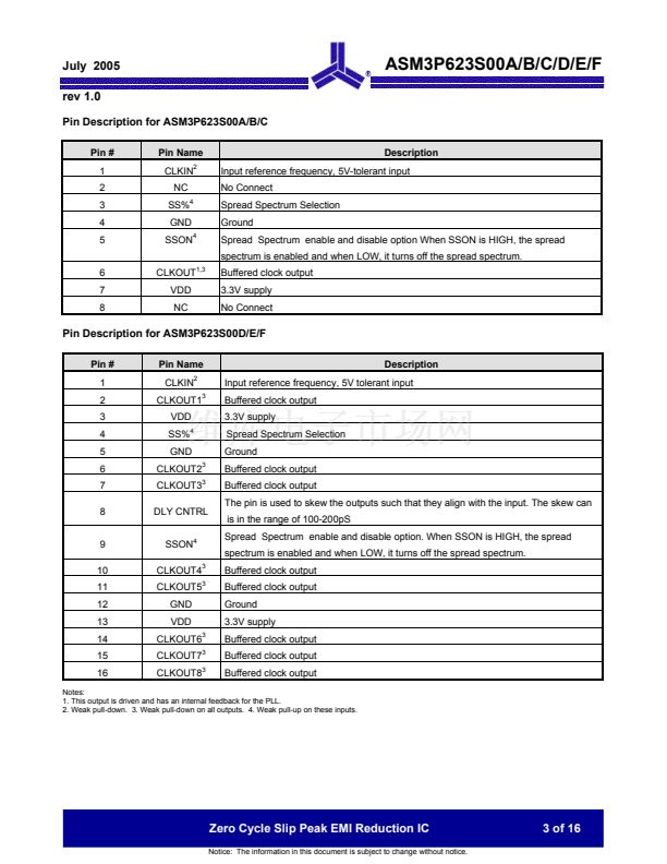
Differential Cycle Slips and Spread Spectrum Control Table
(Note: The values given in the table are for an input frequency of 32 MHz)
ASM3P623S00A/B/C/D/E/F
Device
ASM3P623S00A
SS%
0
1
0
1
0
1
0
1
0
1
0
1
Deviation
鹵0.5 %
鹵1 %
鹵0.25 %
鹵0.5 %
鹵0.125 %
鹵0.25 %
鹵0.5 %
鹵1 %
鹵0.25 %
鹵0.5 %
鹵0.125 %
鹵0.25 %
Differential Cycle Slips
(Nd)
0.125
0.25
0.125
0.25
0.125
0.25
0.125
0.25
0.125
0.25
0.125
0.25
ASM3P623S00B
ASM3P623S00C
ASM3P623S00D
ASM3P623S00E
ASM3P623S00F
Absolute Maximum Ratings
Parameter
Supply Voltage to Ground Potential
DC Input Voltage (Except CLKIN)
DC Input Voltage (CLKIN)
Storage Temperature
Max. Soldering Temperature (10 sec)
Junction Temperature
Static Discharge Voltage
(As per JEDEC STD22- A114-B)
Min
-0.5
-0.5
-0.5
-65
Max
+7.0
VDD + 0.5
7
+150
260
150
2000
Unit
V
V
V
擄C
擄C
擄C
V
Note: These are stress ratings only and functional usage is not implied. Exposure to absolute maximum ratings for prolonged periods can affect device
reliability.
Zero Cycle Slip Peak EMI Reduction IC
Notice: The information in this document is subject to change without notice.
4 of 16


 1
1
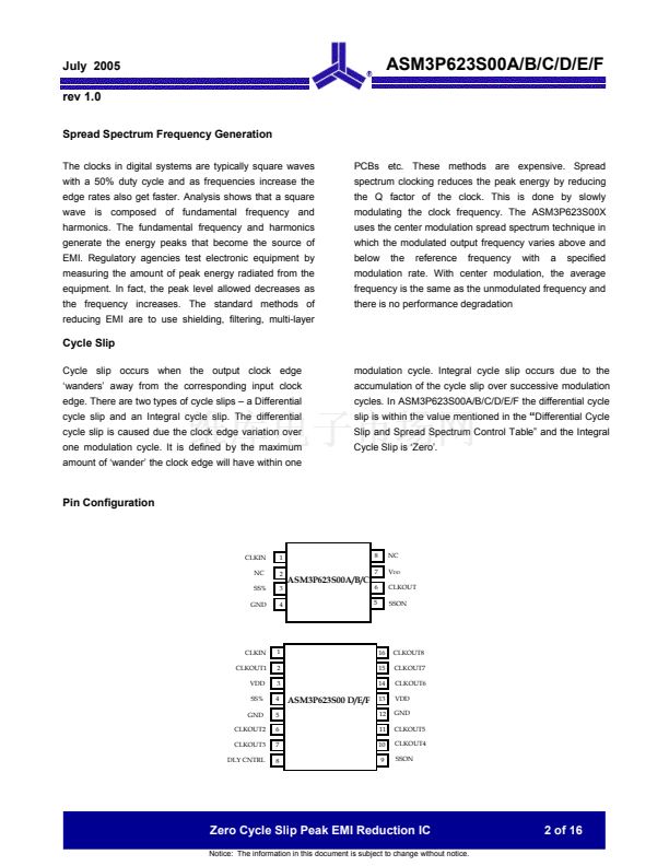 2
2
 3
3
 4
4
 5
5
 6
6
 7
7
 8
8
 9
9
 10
10
 11
11
 12
12
 13
13
 14
14
 15
15
 16
16
