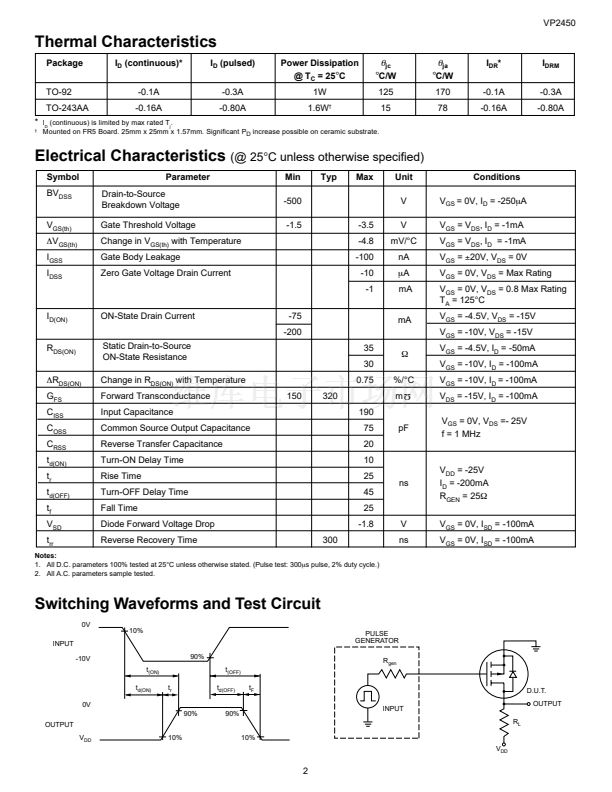
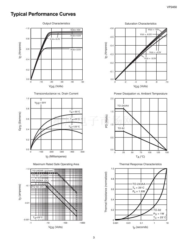
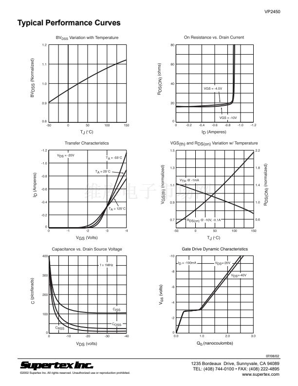
VP2450
Typical Performance Curves
BV
DSS
Variation with Temperature
1.2
80
On Resistance vs. Drain Current
BVDSS (Normalized)
RDS(ON) (ohms)
1.1
60
1.0
40
VGS = -4.5V
0.9
20
VGS = -10V
0.8
-50
0
50
100
150
0
0
-0.2
-0.4
-0.6
-0.8
-1.0
-1.2
TJ (
擄
C)
Transfer Characteristics
-1.2
VDS = -20V
-1.0
TA = 25
擄
C
-0.8
TA = -55
擄
C
ID (Amperes)
VGS(th) and RDS(on) Variation w/ Temperature
1.5
2.2
1.3
1.8
VTH @ -1mA
1.1
1.4
-0.6
-0.4
TA = 125
擄
C
-0.2
0.9
1.0
0.7
0
0
-1
-2
-3
-4
-50
RDS(on) @ -10V, -0.1A
0.6
0
50
100
150
VGS (Volts)
TJ (
擄
C)
Gate Drive Dynamic Characteristics
-10
ID = -100mA
-8
VDS=-20V
Capacitance vs. Drain Source Voltage
400
f = 1MHz
300
C (picofarads)
VDS=-40V
V
GS
(volts)
-6
200
-4
CISS
100
-2
COSS
0
0
-10
-20
-30
-40
0.0
1.0
2.0
3.0
CRSS
0
VDS (volts)
Q
G
(nanocoulombs)
漏2002 Supertex Inc. All rights reserved. Unauthorized use or reproduction prohibited.
4
1235 Bordeaux Drive, Sunnyvale, CA 94089
TEL: (408) 744-0100 鈥?FAX: (408) 222-4895
www.supertex.com
RDS(ON) (normalized)
VGS(th) (normalized)
ID (Amperes)
07/08/02


 1
1
 2
2
 3
3
 4
4
