鈥?/div>
Mounted on FR5 board, 25mm x 25mm x 1.57mm. Significant P increase possible on ceramic substrate.
D
I
D
(continuous) is limited by max rated T
j
.
Electrical Characteristics
(@ 25擄C unless otherwise specified)
Symbol
BV
DSS
V
GS(th)
鈭哣
GS(th)
I
GSS
I
DSS
Parameter
Drain-to-Source
Breakdown Voltage
Gate Threshold Voltage
Change in V
GS(th)
with Temperature
Gate Body Leakage
Zero Gate Voltage Drain Current
Min
40
0.6
-3.8
1.6
-4.5
100
10
1
I
D(ON)
R
DS(ON)
鈭哛
DS(ON)
G
FS
C
ISS
C
OSS
C
RSS
t
d(ON)
t
r
t
d(OFF)
t
f
V
SD
t
rr
ON-State Drain Current
1.0
4.0
Static Drain-to-Source
ON-State Resistance
Change in R
DS(ON)
with Temperature
Forward Transconductance
Input Capacitance
Common Source Output Capacitance
Reverse Transfer Capacitance
Turn-ON Delay Time
Rise Time
Turn-OFF Delay Time
Fall Time
Diode Forward Voltage Drop
Reverse Recovery Time
1.2
300
0.5
0.7
70
50
20
125
70
25
10
10
25
13
1.8
V
ns
V
GS
= 0V, I
SD
= 1.5A
V
GS
= 0V, I
SD
= 1A
ns
V
DD
= 20V,
I
D
= 500mA,
R
GEN
= 25鈩?/div>
pF
1.7
4.5
1.25
0.8
1.5
1.0
0.75
%/擄C
鈩?/div>
Typ
Max
Unit
V
V
mV/擄C
nA
碌A(chǔ)
mA
A
Conditions
V
GS
= 0V, I
D
= 2mA
V
GS
= V
DS
, I
D
= 1mA
V
GS
= V
DS
, I
D
= 1mA
V
GS
=
鹵
20V, V
DS
= 0V
V
GS
= 0V, V
DS
= Max Rating
V
GS
= 0V, V
DS
= 0.8 Max Rating
T
A
= 125擄C
V
GS
= 5V, V
DS
= 15V
V
GS
= 10V, V
DS
= 15V
V
GS
= 5V, I
D
= 300mA
V
GS
= 10V, I
D
= 1.5A
V
GS
= 10V, I
D
= 1.5A
V
DS
= 15V, I
D
= 2.0A
V
GS
= 0V, V
DS
= 20V
f = 1 MHz
Notes:
1. All D.C. parameters 100% tested at 25擄C unless otherwise stated. (Pulse test: 300碌s pulse, 2% duty cycle.)
2. All A.C. parameters sample tested.
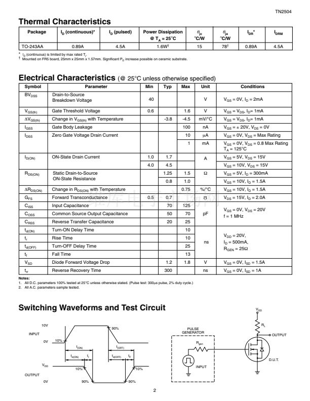
Switching Waveforms and Test Circuit
10V
90%
INPUT
0V
PULSE
GENERATOR
R
gen
10%
t
(ON)
t
(OFF)
t
r
t
d(OFF)
t
F
t
d(ON)
V
DD
10%
10%
INPUT
OUTPUT
0V
90%
90%
2
prev
next


 1
1
 2
2
 3
3
 4
4
