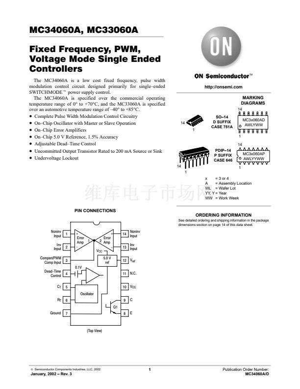
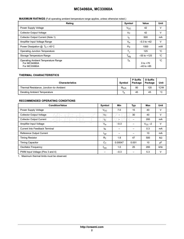
MC34060A, MC33060A
APPLICATIONS INFORMATION
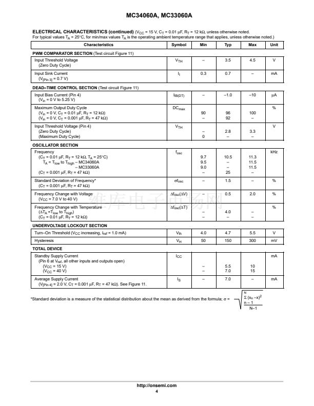
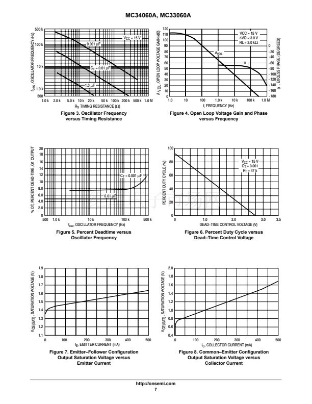
The control signals are external inputs that can be fed into
the dead鈥搕ime control, the error amplifier inputs, or the
feed鈥揵ack input. The dead鈥搕ime control comparator has an
effective 120 mV input offset which limits the minimum
output dead time to approximately the first 4% of the
sawtooth鈥揷ycle time. This would result in a maximum duty
cycle of 96%. Additional dead time may be imposed on the
output by setting the dead time鈥揷ontrol input to a fixed
voltage, ranging between 0 V to 3.3 V.
The pulse width modulator comparator provides a means
for the error amplifiers to adjust the output pulse width from
the maximum percent on鈥搕ime, established by the dead time
control input, down to zero, as the voltage at the feedback
pin varies from 0.5 V to 3.5 V. Both error amplifiers have a
common mode input range from 鈥?.3 V to (V
CC
鈥?.0 V), and
may be used to sense power supply output voltage and
current. The error鈥揳mplifier outputs are active high and are
ORed together at the noninverting input of the pulse鈥搘idth
modulator comparator. With this configuration, the
amplifier that demands minimum output on time, dominates
control of the loop.
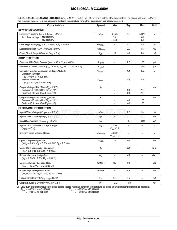
The MC34060A has an internal 5.0 V reference capable
of sourcing up to 10 mA of load currents for external bias
circuits. The reference has an internal accuracy of
鹵5%
with
a typical thermal drift of less than 50 mV over an operating
temperature range of 0擄 to +70擄C.
http://onsemi.com
6


 1
1
 2
2
 3
3
 4
4
 5
5
 6
6
 7
7
 8
8
 9
9
 10
10
 11
11
 12
12
 13
13
 14
14
 15
15
 16
16
