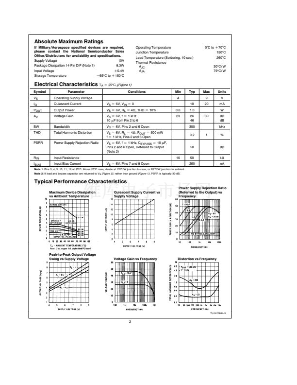
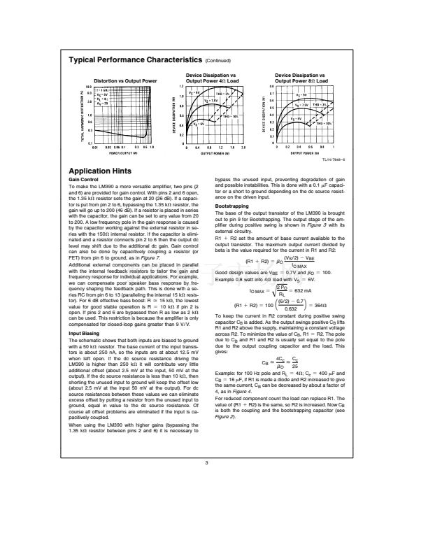
Typical Performance Characteristics
Distortion vs Output Power
(Continued)
Device Dissipation vs
Output Power 8X Load
Device Dissipation vs
Output Power 4X Load
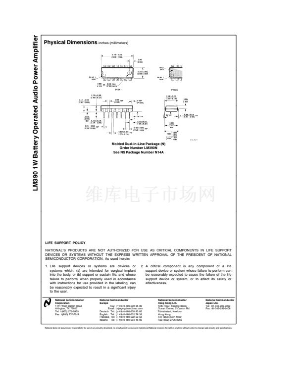
TL H 7848 鈥?6
Application Hints
Gain Control
To make the LM390 a more versatile amplifier two pins (2
and 6) are provided for gain control With pins 2 and 6 open
the 1 35 kX resistor sets the gain at 20 (26 dB) If a capaci-
tor is put from pin 2 to 6 bypassing the 1 35 kX resistor the
gain will go up to 200 (46 dB) If a resistor is placed in series
with the capacitor the gain can be set to any value from 20
to 200 A low frequency pole in the gain response is caused
by the capacitor working against the external resistor in se-
ries with the 150X internal resistor If the capacitor is elimi-
nated and a resistor connects pin 2 to 6 then the output dc
level may shift due to the additional dc gain Gain control
can also be done by capacitively coupling a resistor (or
FET) from pin 6 to ground as in
Figure 7
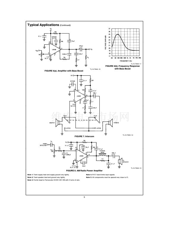
Additional external components can be placed in parallel
with the internal feedback resistors to tailor the gain and
frequency response for individual applications For example
we can compensate poor speaker bass response by fre-
quency shaping the feedback path This is done with a se-
ries RC from pin 6 to 13 (paralleling the internal 15 kX resis-
tor) For 6 dB effective bass boost R
j
15 kX the lowest
value for good stable operation is R
e
10 kX if pin 2 is
open If pins 2 and 6 are bypassed then R as low as 2 kX
can be used This restriction is because the amplifier is only
compensated for closed-loop gains greater than 9 V V
Input Biasing
The schematic shows that both inputs are biased to ground
with a 50 kX resistor The base current of the input transis-
tors is about 250 nA so the inputs are at about 12 5 mV
when left open If the dc source resistance driving the
LM390 is higher than 250 kX it will contribute very little
additional offset (about 2 5 mV at the input 50 mV at the
output) If the dc source resistance is less than 10 kX then
shorting the unused input to ground will keep the offset low
(about 2 5 mV at the input 50 mV at the output) For dc
source resistances between these values we can eliminate
excess offset by putting a resistor from the unused input to
ground equal in value to the dc source resistance Of
course all offset problems are eliminated if the input is ca-
pacitively coupled
When using the LM390 with higher gains (bypassing the
1 35 kX resistor between pins 2 and 6) it is necessary to
bypass the unused input preventing degradation of gain
and possible instabilities This is done with a 0 1
mF
capaci-
tor or a short to ground depending on the dc source resist-
ance on the driven input
Bootstrapping
The base of the output transistor of the LM390 is brought
out to pin 9 for Bootstrapping The output stage of the am-
plifier during positive swing is shown in
Figure 3
with its
external circuitry
R1
a
R2 set the amount of base current available to the
output transistor The maximum output current divided by
beta is the value required for the current in R1 and R2
(R1
a
R2)
e
b
O
(V
S
2)
b
V
BE
I
O MAX
Good design values are V
BE
e
0 7V and
b
O
e
100
Example 0 8 watt into 4X load with V
S
e
6V
2 P
O
e
632 mA
I
O MAX
e
R
L
(6 2)
b
0 7
e
364X
(R1
a
R2)
e
100
0 632
To keep the current in R2 constant during positive swing
capacitor C
B
is added As the output swings positive C
B
lifts
R1 and R2 above the supply maintaining a constant voltage
across R2 To minimize the value of C
B
R1
e
R2 The pole
due to C
B
and R1 and R2 is usually set equal to the pole
due to the output coupling capacitor and the load This
gives
4C
c
C
j
c
b
O
25
e
4X C
c
e
400
mF
and
Example for 100 Hz pole and R
L
C
B
e
16
mF
if R1 is made a diode and R2 increased to give
the same current C
B
can be decreased by about a factor of
4 as in
Figure 4
For reduced component count the load can replace R1 The
value of (R1
a
R2) is the same so R2 is increased Now C
B
is both the coupling and the bootstrapping capacitor (see
Figure 2
)
C
B
j
0
�
J
3


 1
1
 2
2
 3
3
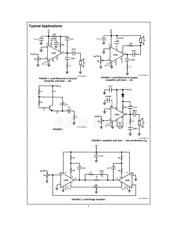 4
4
 5
5
 6
6
