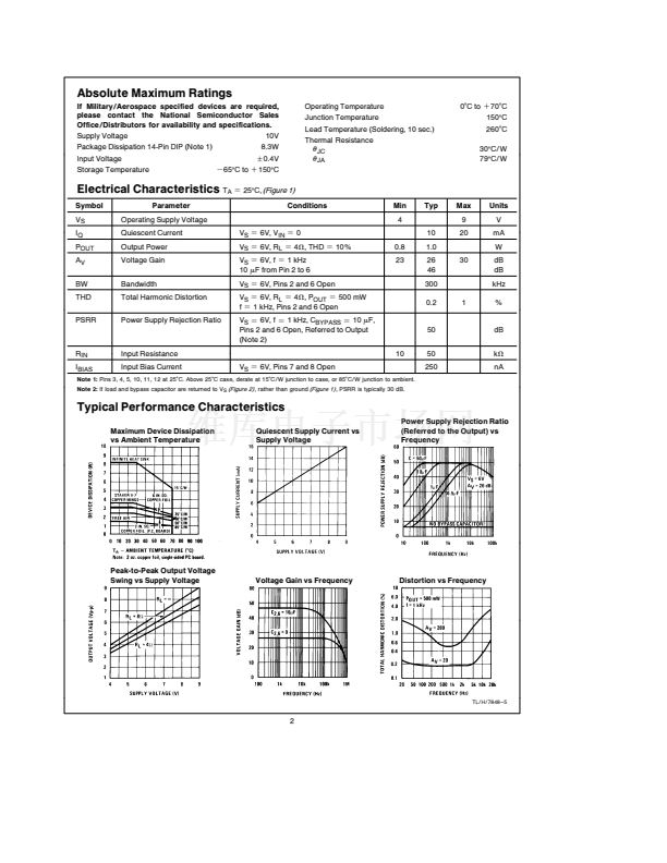
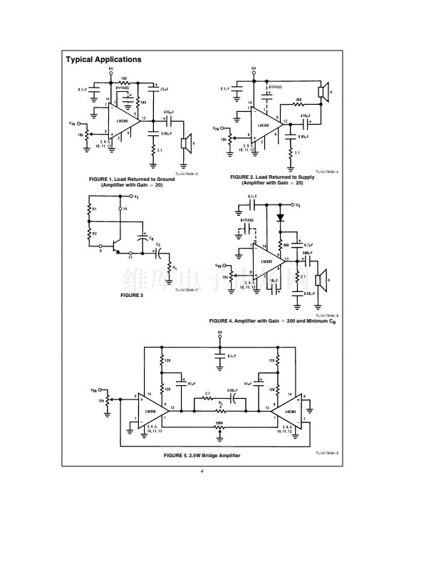
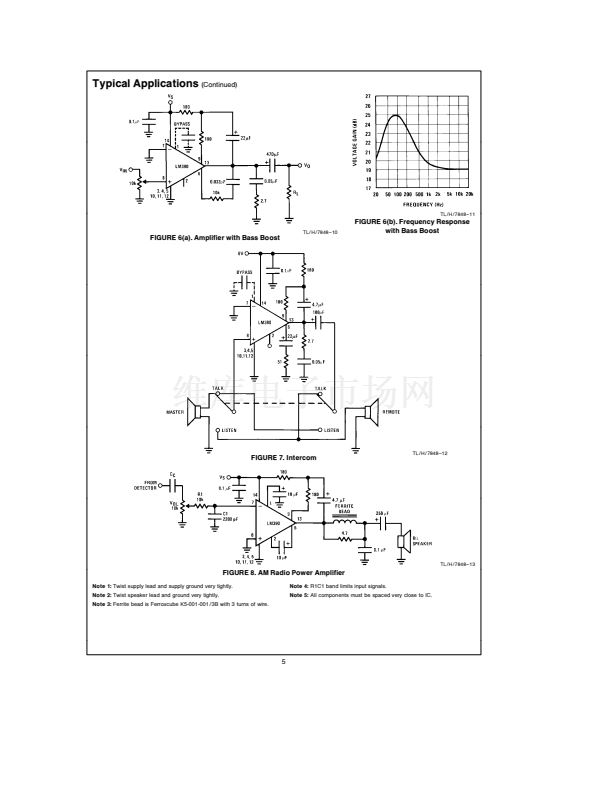
Absolute Maximum Ratings
If Military Aerospace specified devices are required
please contact the National Semiconductor Sales
Office Distributors for availability and specifications
Supply Voltage
Package Dissipation 14-Pin DIP (Note 1)
Input Voltage
Storage Temperature
10V
8 3W
g
0 4V
Operating Temperature
Junction Temperature
Lead Temperature (Soldering 10 sec )
Thermal Resistance
i
JC
i
JA
0 C to
a
70 C
150 C
260 C
30 C W
79 C W
b
65 C to
a
150 C
Electrical Characteristics
T
A
e
25 C
(Figure 1)
Symbol
V
S
I
Q
P
OUT
A
V
BW
THD
PSRR
Parameter
Operating Supply Voltage
Quiescent Current
Output Power
Voltage Gain
Bandwidth
Total Harmonic Distortion
Power Supply Rejection Ratio
V
S
e
6V V
IN
e
0
V
S
e
6V R
L
e
4X THD
e
10%
V
S
e
6V f
e
1 kHz
10
mF
from Pin 2 to 6
V
S
e
6V Pins 2 and 6 Open
V
S
e
6V R
L
e
4X P
OUT
e
500 mW
f
e
1 kHz Pins 2 and 6 Open
V
S
e
6V f
e
1 kHz C
BYPASS
e
10
mF
Pins 2 and 6 Open Referred to Output
(Note 2)
10
V
S
e
6V Pins 7 and 8 Open
08
23
Conditions
Min
4
10
10
26
46
300
02
1
30
Typ
Max
9
20
Units
V
mA
W
dB
dB
kHz
%
50
50
250
dB
kX
nA
R
IN
I
BIAS
Input Resistance
Input Bias Current
Note 1
Pins 3 4 5 10 11 12 at 25 C Above 25 C case derate at 15 C W junction to case or 85 C W junction to ambient
Note 2
If load and bypass capacitor are returned to V
S
(Figure 2)
rather than ground
(Figure 1)
PSRR is typically 30 dB
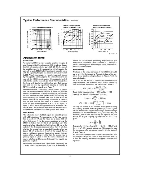
Typical Performance Characteristics
Maximum Device Dissipation
vs Ambient Temperature
Quiescent Supply Current vs
Supply Voltage
Power Supply Rejection Ratio
(Referred to the Output) vs
Frequency
Peak-to-Peak Output Voltage
Swing vs Supply Voltage
Voltage Gain vs Frequency
Distortion vs Frequency
TL H 7848 鈥?5
2


 1
1
 2
2
 3
3
 4
4
 5
5
 6
6
