鈥?/div>
+ 0.540
90
UNITS
V
V
V
V
V
V
mA
碌A(chǔ)
The
q
denotes specifications which apply over the full operating
temperature range.
Note 1:
A heat sink may be required to keep the junction temperature below
the Absolute Maximum Rating when the output is shorted indefinitely.
Note 2:
This parameter is not 100% tested.
Note 3:
Input offset match is the difference in offset voltage between
amplifiers measured at both V
CM
= V
鈥?/div>
and V
CM
= V
+
.
Note 4:
Matching parameters are the difference between amplifiers A and
D and between B and C.
TYPICAL PERFORMANCE CHARACTERISTICS
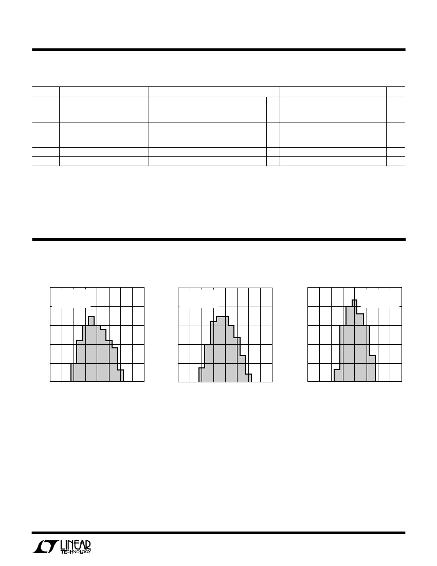
V
OS
Distribution, V
CM
= 0V
25
V
S
= 5V, 0V
V
CM
= 0V
1900 AMPLIFIERS
25
V
S
= 5V, 0V
V
CM
= 5V
1900 AMPLIFIERS
20
PERCENT OF UNITS (%)
15
PERCENT OF UNITS (%)
PERCENT OF UNITS (%)
10
5
0
鈥?400 鈥?300 鈥?200 鈥?00 0 100 200 300 400
INPUT OFFSET VOLTAGE (碌V)
1466L/67L G01
U W
V
OS
Distribution, V
CM
= 5V
25
V
OS
Shift, V
CM
= 0V to 5V
V
S
= 5V, 0V
V
CM
= 0V TO 5V
1900 AMPLIFIERS
20
15
20
15
10
10
5
5
0
鈥?400 鈥?300 鈥?200 鈥?00 0
100 200 300 400
INPUT OFFSET VOLTAGE (碌V)
1466L/67L G02
0
鈥?400 鈥?300 鈥?200 鈥?00 0 100 200 300 400
INPUT OFFSET VOLTAGE SHIFT (碌V)
1466L/67L G03
5


 1
1
 2
2
 3
3
 4
4
 5
5
 6
6
 7
7
 8
8
 9
9
 10
10
 11
11
 12
12
