SLUS507C 鈭?JANUARY 2002 鈭?REVISED JUNE 2004
TPS40000, TPS40001
TPS40002, TPS40003
TPS40004, TPS40005
APPLICATION INFORMATION
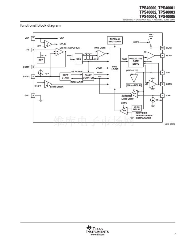
error amplifier
The error amplifier has a bandwidth of greater than 5 MHz, with open loop gain of at least 55 dB. The COMP
output voltage is clamped to a level above the oscillator ramp in order to improve large-scale transient response.
oscillator
The oscillator uses an internal resistor and capacitor to set the oscillation frequency. The ramp waveform is a
triangle at the PWM frequency with a peak voltage of 1.25 V, and a valley of 0.25 V. The PWM duty cycle is limited
to a maximum of 95%, allowing the bootstrap capacitor to charge during every cycle.
bootstrap/charge pump
There is an internal switch between VDD and BOOT. This switch charges the external bootstrap capacitor for
the floating supply. If the resistance of this switch is too high for the application, an external schottky diode
between VDD and BOOT can be used. The peak voltage on the bootstrap capacitor is approximately equal to
VDD.
driver
The HDRV and LDRV MOSFET drivers are capable of driving gate-to-source voltages up to 5.5 V. At V
IN
, = 5 V
and using appropriate MOSFETs, a 20-A converter can be achieved. The LDRV driver switches between VDD
and ground, while the HDRV driver is referenced to SW and switches between BOOT and SW. The maximum
voltage between BOOT and SW is 5.5 V.
synchronous rectification and predictive delay
In a normal buck converter, when the main switch turns off, current is flowing to the load in the inductor. This
current cannot be stopped immediately without using infinite voltage. For the current path to flow and maintain
voltage levels at a safe level, a rectifier or catch device is used. This device can be either a conventional diode,
or it can be a controlled active device if a control signal is available to drive it. The TPS4000x provides a signal
to drive an N-channel MOSFET as a rectifier. This control signal is carefully coordinated with the drive signal
for the main switch so that there is minimum delay from the time that the rectifier MOSFET turns off and the main
switch turns on, and minimum delay from when the main switch turns off and the rectifier MOSFET turns on.
This scheme, Predictive Gate Drivet delay, uses information from the current switching cycle to adjust the
delays that are to be used in the next cycle. Figure 2 shows the switch-node voltage waveform for a
synchronously rectified buck converter. Illustrated are the relative effects of a fixed-delay drive scheme
(constant, pre-set delays for the turn-off to turn-on intervals), an adaptive delay drive scheme (variable delays
based upon voltages sensed on the current switching cycle) and the predictive delay drive scheme.
Note that the longer the time spent in diode conduction during the rectifier conduction period, the lower the
efficiency. Also, not described in Figure 2 is the fact that the predictive delay circuit can prevent the body diode
from becoming forward biased at all while at the same time avoiding cross conduction or shoot through. This
results in a significant power savings when the main MOSFET turns on, and minimizes reverse recovery loss
in the body diode of the rectifier MOSFET.
www.ti.com
9


 1
1
 2
2
 3
3
 4
4
 5
5
 6
6
 7
7
 8
8
 9
9
 10
10
 11
11
 12
12
 13
13
 14
14
 15
15
 16
16
 17
17
 18
18
 19
19
 20
20
