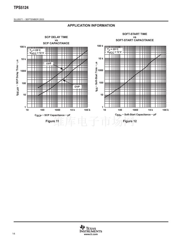
TPS5124
SLUS571 鈭?SEPTEMBER 2003
FUNCTIONAL DESCRIPTION
INPUT VOLTAGE RANGE
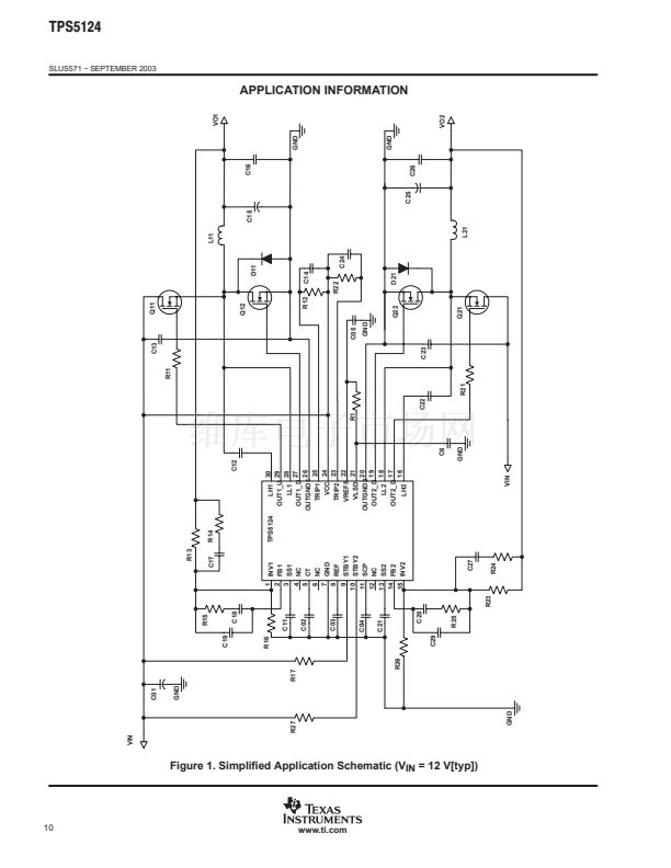
TPS5124 supports two input voltage ranges. When V
VCC
is between 6.5 V and 15 V, VLSD is connected to
VREF5 with R-C filter (see Figure 1). When V
VCC
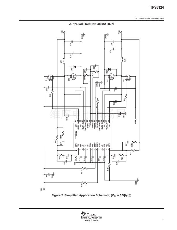
is between 4.5 V and 5.5 V, VLSD is connected to VCC with
R-C filter and VREF5 is connected to VCC. (see Figure2).
REFERENCE VOLTAGE (0.85 V)
This 0.85-V reference voltage is used to set the output voltage and the reference for the overvoltage and
undervoltage protections. This reference voltage is dropped down from the internal
5V
regulator.
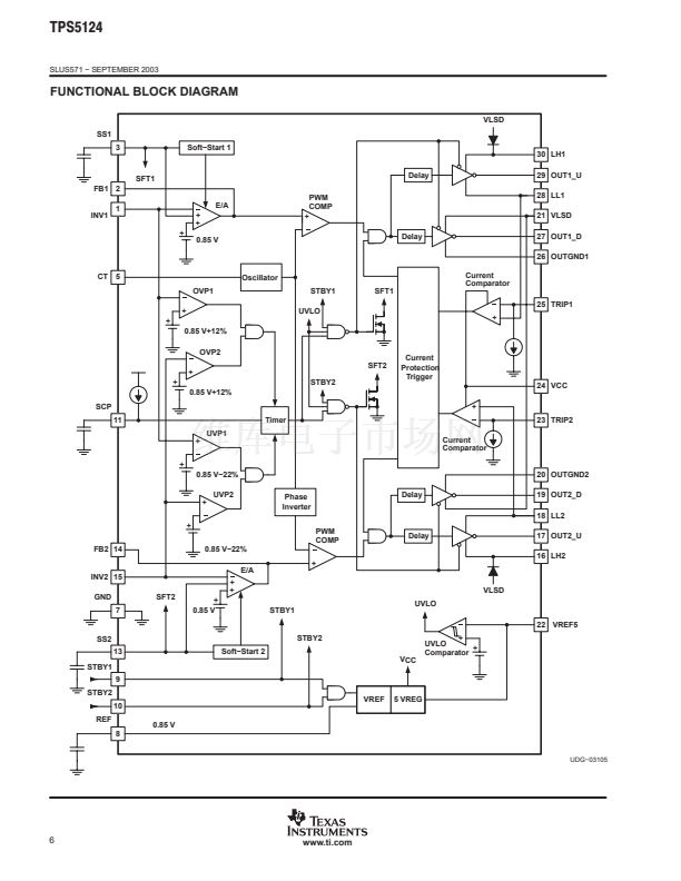
PWM OPERATION
TPS5124 includes dual synchronous buck regulator controllers (SBRC) that operate 180_ out of phase and
same frequency. Both channels have individual standby and softstart controller.
5-V REGULATOR
An internal linear voltage regulator is used for the reference voltage and power supply of internal circuit. When
this regulator is connected to the VLSD pin, it is used for powering the low-side driver and powering the high-side
driver through the built-in bootstrap diode or external bootstrap circuit. It is active if either STBY1 or STBY2 is
HIGH and has a tolerance of 4 %.
ERROR AMPLIFIER
Each channel has its own error amplifier to regulate the output voltage of the synchronous buck converter. The
unity gain bandwidth is 2.5 MHz. This decreases the amplifier delay during fast load transients and contributes
to a fast transient response.
LOW-SIDE DRIVER
The low-side driver is designed to drive high current and low R
DS(on)
N-channel MOSFET(s). The maximum
drive voltage is 5 V from the VLSD pin. The current rating of the driver is typically 1.5 A at source and sink.
HIGH-SIDE DRIVER
The high-side driver is designed to drive high current and low R
DS(on)
N鈭抍hannel MOSFET(s). The current rating
of the driver is 1.2 A (typ.) at source and sink. When configured as a floating driver a bias voltage is delivered
from the VSLD pin through built-in bootstrap diode or external bootstrap circuit. When the MOSFET needs high
gate threshold voltage, it is useful to add the external schottky diodes which provide a higher voltage for the gate
drive than using the built-in diodes. The instantaneous drive current is supplied by the flying capacitor between
the LH and LL pins since a bias power supply does not usually have low impedance. The maximum voltage
between the OUTx_U and LLx pins is about 5.5 V when the VSLD pin is connected to the VREF5 pin. The
maximum voltage that can be applied between the LH and OUTGND pins is 22 V.
DEAD-TIME
The internally defined dead-time prevents shoot-through current flowing through the main power MOSFETs
during switching transitions.
www.ti.com
7


 1
1
 2
2
 3
3
 4
4
 5
5
 6
6
 7
7
 8
8
 9
9
 10
10
 11
11
 12
12
 13
13
 14
14
 15
15
 16
16
