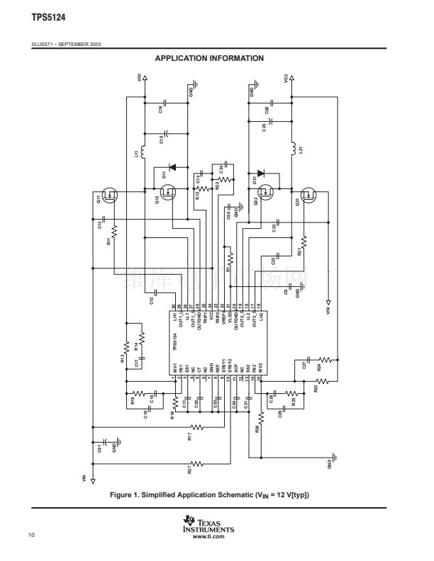
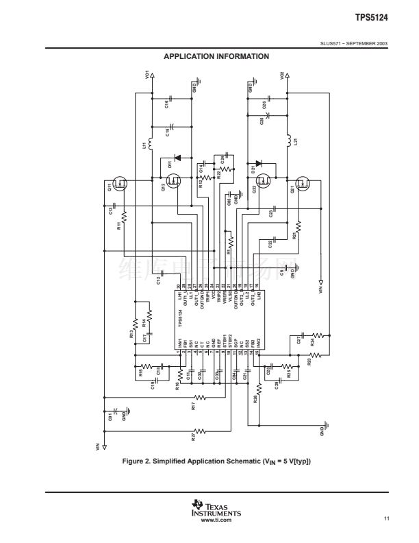
鈭?/div>
O
I/O
I/O
I/O
I
I
I
I
I
I
O
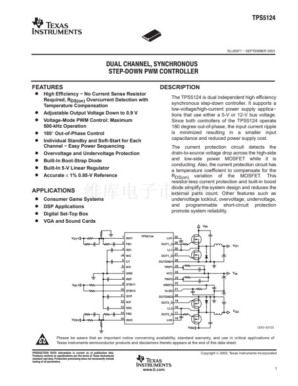
DESCRIPTION
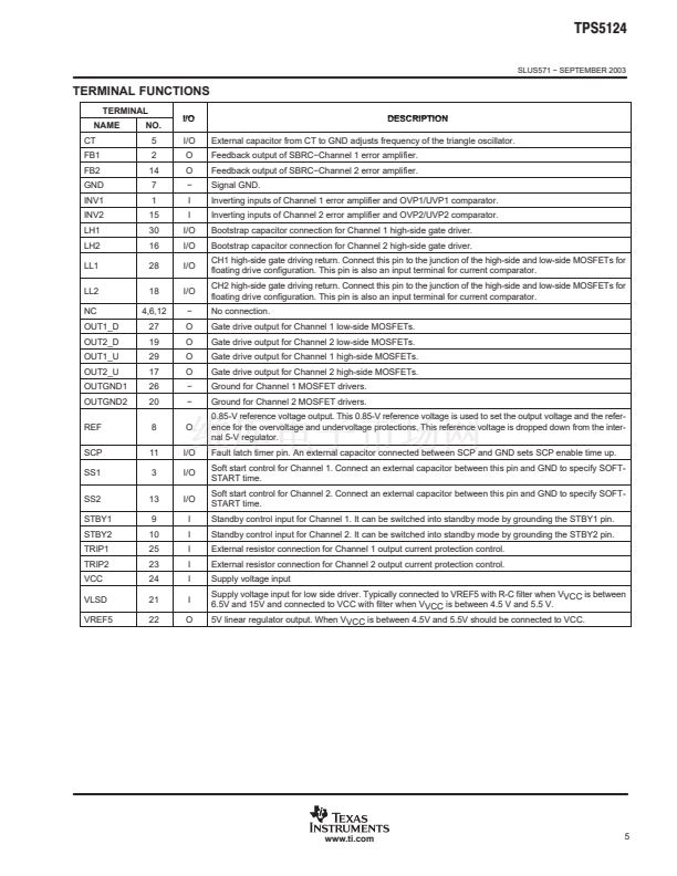
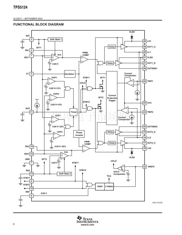
External capacitor from CT to GND adjusts frequency of the triangle oscillator.
Feedback output of SBRC鈭扖hannel 1 error amplifier.
Feedback output of SBRC鈭扖hannel 2 error amplifier.
Signal GND.
Inverting inputs of Channel 1 error amplifier and OVP1/UVP1 comparator.
Inverting inputs of Channel 2 error amplifier and OVP2/UVP2 comparator.
Bootstrap capacitor connection for Channel 1 high-side gate driver.
Bootstrap capacitor connection for Channel 2 high-side gate driver.
CH1 high-side gate driving return. Connect this pin to the junction of the high-side and low-side MOSFETs for
floating drive configuration. This pin is also an input terminal for current comparator.
CH2 high-side gate driving return. Connect this pin to the junction of the high-side and low-side MOSFETs for
floating drive configuration. This pin is also an input terminal for current comparator.
No connection.
Gate drive output for Channel 1 low-side MOSFETs.
Gate drive output for Channel 2 low-side MOSFETs.
Gate drive output for Channel 1 high-side MOSFETs.
Gate drive output for Channel 2 high-side MOSFETs.
Ground for Channel 1 MOSFET drivers.
Ground for Channel 2 MOSFET drivers.
0.85-V reference voltage output. This 0.85-V reference voltage is used to set the output voltage and the refer-
ence for the overvoltage and undervoltage protections. This reference voltage is dropped down from the inter-
nal 5-V regulator.
Fault latch timer pin. An external capacitor connected between SCP and GND sets SCP enable time up.
Soft start control for Channel 1. Connect an external capacitor between this pin and GND to specify SOFT-
START time.
Soft start control for Channel 2. Connect an external capacitor between this pin and GND to specify SOFT-
START time.
Standby control input for Channel 1. It can be switched into standby mode by grounding the STBY1 pin.
Standby control input for Channel 2. It can be switched into standby mode by grounding the STBY2 pin.
External resistor connection for Channel 1 output current protection control.
External resistor connection for Channel 2 output current protection control.
Supply voltage input
Supply voltage input for low side driver. Typically connected to VREF5 with R-C filter when VVCC is between
6.5V and 15V and connected to VCC with filter when VVCC is between 4.5 V and 5.5 V.
5V linear regulator output. When VVCC is between 4.5V and 5.5V should be connected to VCC.
www.ti.com
5


 1
1
 2
2
 3
3
 4
4
 5
5
 6
6
 7
7
 8
8
 9
9
 10
10
 11
11
 12
12
 13
13
 14
14
 15
15
 16
16
