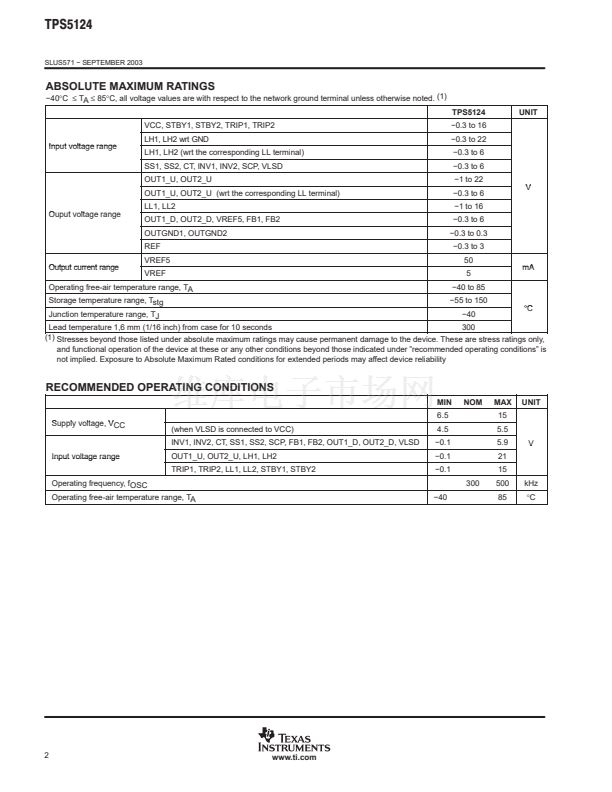
鈮?/div>
85擄C, all voltage values are with respect to the network ground terminal unless otherwise noted. (1)
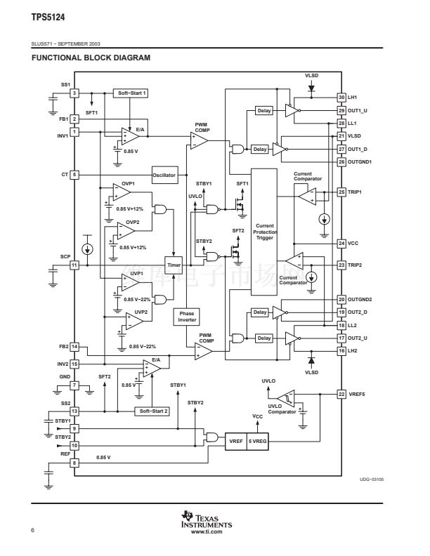
TPS5124
VCC, STBY1, STBY2, TRIP1, TRIP2
LH1, LH2 wrt GND
Input voltage range
LH1, LH2 (wrt the corresponding LL terminal)
SS1, SS2, CT, INV1, INV2, SCP, VLSD
OUT1_U, OUT2_U
OUT1_U, OUT2_U (wrt the corresponding LL terminal)
LL1, LL2
Ouput voltage range
OUT1_D, OUT2_D, VREF5, FB1, FB2
OUTGND1, OUTGND2
REF
VREF5
Output current range
VREF
Operating free-air temperature range, TA
Storage temperature range, Tstg
Junction temperature range, TJ
鈭?.3 to 16
鈭?.3 to 22
鈭?.3 to 6
鈭?.3 to 6
鈭? to 22
鈭?.3 to 6
鈭? to 16
鈭?.3 to 6
鈭?.3 to 0.3
鈭?.3 to 3
50
5
鈭?0 to 85
鈭?5 to 150
鈭?0
擄C
mA
V
UNIT
Lead temperature 1,6 mm (1/16 inch) from case for 10 seconds
300
(1) Stresses beyond those listed under absolute maximum ratings may cause permanent damage to the device. These are stress ratings only,
and functional operation of the device at these or any other conditions beyond those indicated under 鈥漴ecommended operating conditions鈥?is
not implied. Exposure to Absolute Maximum Rated conditions for extended periods may affect device reliability
RECOMMENDED OPERATING CONDITIONS
MIN
6.5
Supply voltage, VCC
(when VLSD is connected to VCC)
INV1, INV2, CT, SS1, SS2, SCP, FB1, FB2, OUT1_D, OUT2_D, VLSD
Input voltage range
Operating frequency, fOSC
Operating free-air temperature range, TA
鈭?0
OUT1_U, OUT2_U, LH1, LH2
TRIP1, TRIP2, LL1, LL2, STBY1, STBY2
4.5
鈭?.1
鈭?.1
鈭?.1
300
NOM
MAX
15
5.5
5.9
21
15
500
85
kHz
擄C
V
UNIT
2
www.ti.com


 1
1
 2
2
 3
3
 4
4
 5
5
 6
6
 7
7
 8
8
 9
9
 10
10
 11
11
 12
12
 13
13
 14
14
 15
15
 16
16
