Low-Voltage SPI/3-Wire RTCs with
Trickle Charger
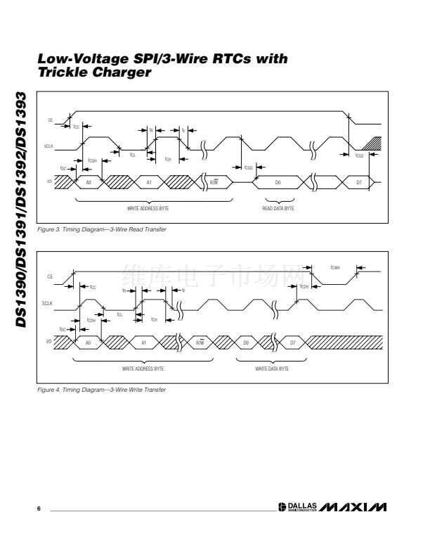
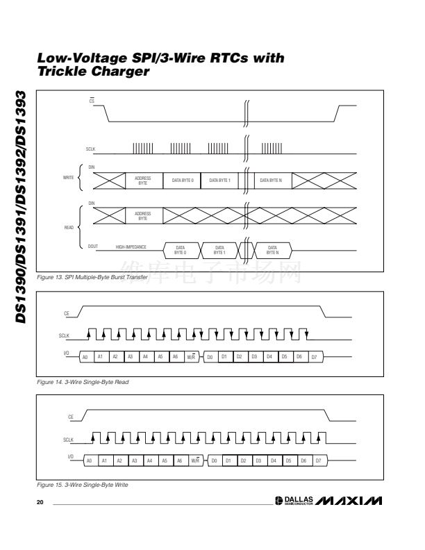
3-Wire Serial-Data Bus
The DS1392/DS1393 provide a 3-wire serial-data bus,
and support both single-byte and multiple-byte data
transfers for maximum flexibility. The I/O pin is the seri-
al-data input/output pin. The CE input is used to initiate
and terminate a data transfer. The SCLK pin is used to
synchronize data movement between the master
(microcontroller) and the slave (DS1392/DS1393)
devices. Input data is latched on the SCLK rising edge
and output data is shifted out on the SCLK falling edge.
There is one clock for each bit transferred. Address
and data bits are transferred in groups of eight.
Address and data bytes are shifted LSB first into the
I/O pin. Data is transferred out LSB first on the I/O pin
for a read operation.
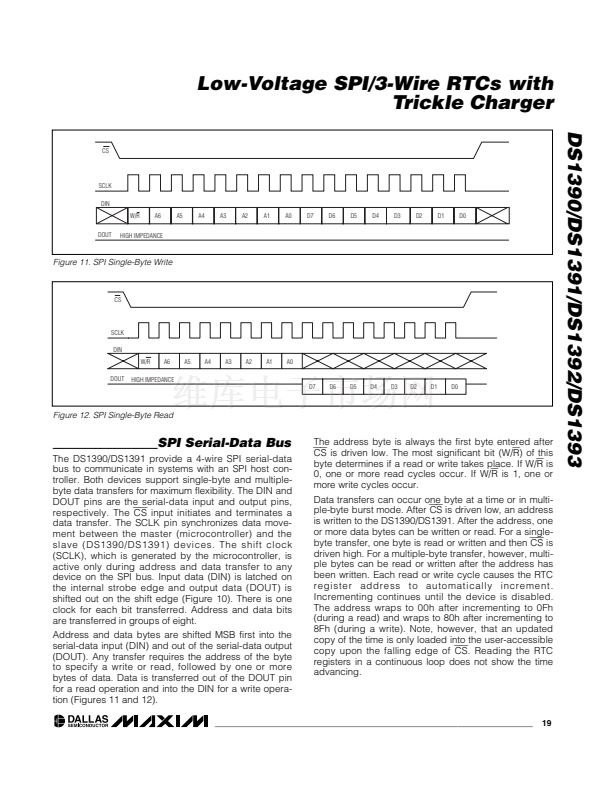
The address byte is always the first byte entered after
CE is driven high. The MSB (W/R) of this byte deter-
mines if a read or write takes place. If W/R is 0, one or
more read cycles occur. If W/R is 1, one or more write
cycles occur.
Data transfers can be one byte at a time or in multiple-
byte burst mode. After CE is driven high, an address is
written to the DS1392/DS1393. After the address, one
or more data bytes can be written or read. For a single-
byte transfer, one byte is read or written and then CE is
driven low (Figure 14 and 15). For a multiple-byte trans-
fer, however, multiple bytes can be read or written after
the address has been written (Figure 16). Each read or
write cycle causes the RTC register address to auto-
matically increment. Incrementing continues until the
device is disabled. The address wraps to 00h after
CE
DS1390/DS1391/DS1392/DS1393
SCLK
I/O
ADDRESS DATA
BYTE
BYTE 0
DATA
BYTE 1
DATA
BYTE N
Figure 16. 3-Wire Multiple-Byte Burst Transfer
incrementing to 0Fh (during a read) and wraps to 80h
after incrementing to 8Fh (during a write). Note, howev-
er, that an updated copy of the time is only loaded into
the user-accessible copy upon the rising edge of CE.
Reading the RTC registers in a continuous loop does
not show the time advancing.
Chip Information
TRANSISTOR COUNT: 11,525
PROCESS: CMOS
SUBSTRATE CONNECTED TO GROUND
Thermal Information
Theta-JA: 180擄C/W
Theta-JC: 41.9擄C/W
____________________________________________________________________
21


 1
1
 2
2
 3
3
 4
4
 5
5
 6
6
 7
7
 8
8
 9
9
 10
10
 11
11
 12
12
 13
13
 14
14
 15
15
 16
16
 17
17
 18
18
 19
19
 20
20
 21
21
 22
22
 23
23
 24
24
