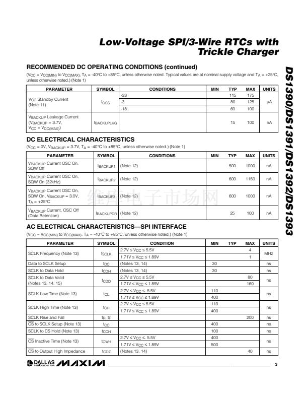
4k鈩?/div>
V
BACKUP
Figure 9. DS1390/DS1391 Programmable Trickle Charger
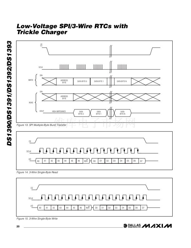
Table 6. SPI Pin Function
CS
MODE
Disable
CSZ
H
SCLK
Input
Disabled
CPOL* = 1,
SCLK Rising
SDI
Input
Disabled
SDO
High
Impedance
DATA LATCH (WRITE/INTERNAL STROBE)
SHIFT DATA OUT (READ)
Write
L
CPOL = 0,
SCLK Falling
CPOL = 1,
SCLK Falling
Data Bit
Latch
High
Impedance
SCLK WHEN CPOL = 0
DATA LATCH (WRITE/INTERNAL STROBE)
SHIFT DATA OUT (READ)
SCLK WHEN CPOL = 1
Read
L
CPOL = 0,
SCLK Rising
X
Next Data
Bit Shift**
NOTE 1:
CPHA BIT POLARITY (IF APPLICABLE) MAY NEED TO BE SET ACCORDINGLY.
NOTE 2:
CPOL IS A BIT SET IN THE MICROCONTROLLER'S CONTROL REGISTER.
NOTE 3:
SDO REMAINS AT HIGH IMPEDANCE UNTIL 8 BITS OF DATA ARE READY TO BE
SHIFTED OUT DURING A READ.
*CPOL
is the clock-polarity bit set in the control register of the
host microprocessor.
**SDO
remains at high impedance until 8 bits of data are ready to
be shifted out during a read.
Figure 10. Serial Clock as a Function of Microcontroller Clock-
Polarity Bit
The user determines diode and resistor selection
according to the maximum current desired for battery
or super cap charging. The maximum charging current
can be calculated as illustrated in the following exam-
ple. Assume that a system power supply of 3.3V is
applied to V
CC
and a super cap is connected to
V
BACKUP
. Also, assume that the trickle charger has
been enabled with a diode and resistor R2 between
V
CC
and V
BACKUP
. The maximum current I
MAX
would
therefore be calculated as follows:
I
MAX
= (3.3V - diode drop) / R2
鈮?/div>
(3.3V - 0.7V) /
2k鈩?/div>
鈮?/div>
1.3mA
As the super cap changes, the voltage drop between
V
CC
and V
BACKUP
decreases and therefore the charge
current decreases.
18
____________________________________________________________________


 1
1
 2
2
 3
3
 4
4
 5
5
 6
6
 7
7
 8
8
 9
9
 10
10
 11
11
 12
12
 13
13
 14
14
 15
15
 16
16
 17
17
 18
18
 19
19
 20
20
 21
21
 22
22
 23
23
 24
24
