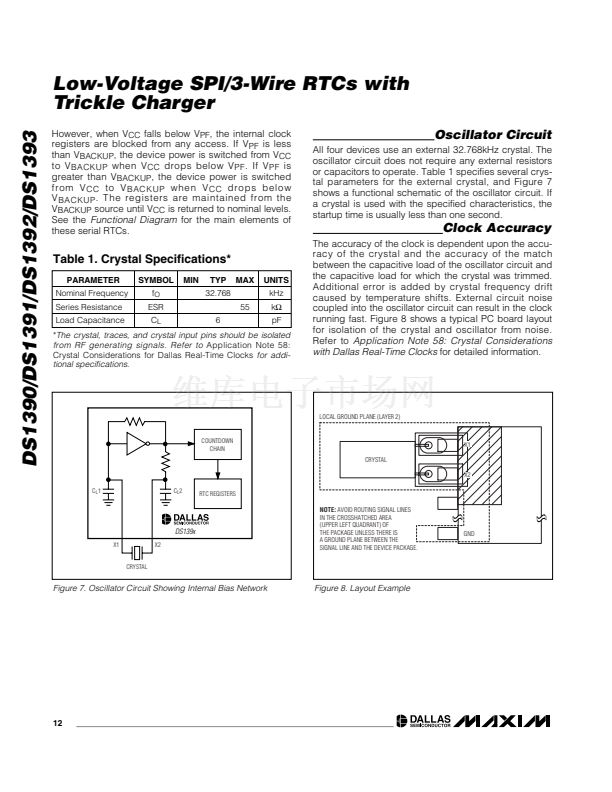
Low-Voltage SPI/3-Wire RTCs with
Trickle Charger
Control Register (0D/8Dh) (DS1392 Only)
BIT 7
EOSC
BIT 6
0
BIT 5
BBSQI
BIT 4
RS2
BIT 3
RS1
BIT 2
ESQW
BIT 1
0
BIT 0
AIE
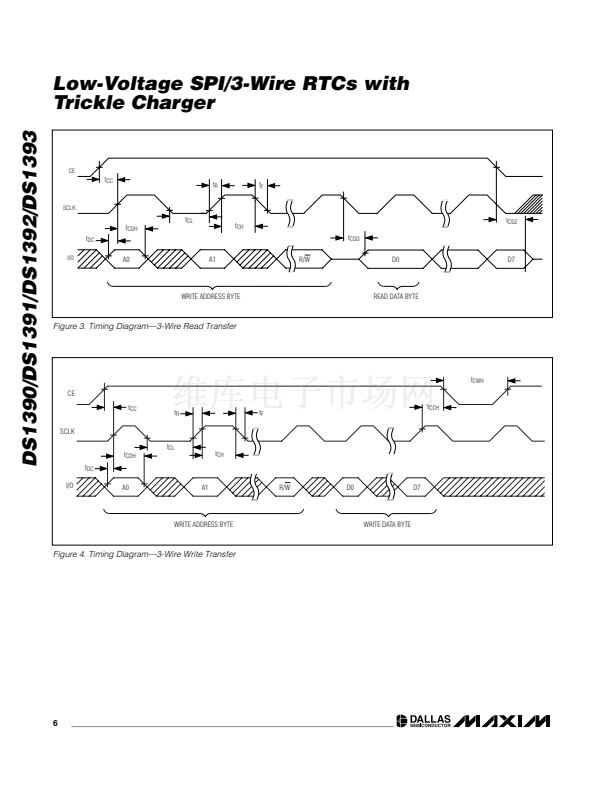
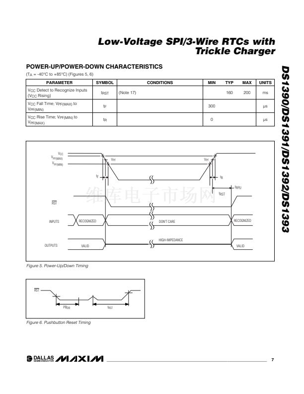
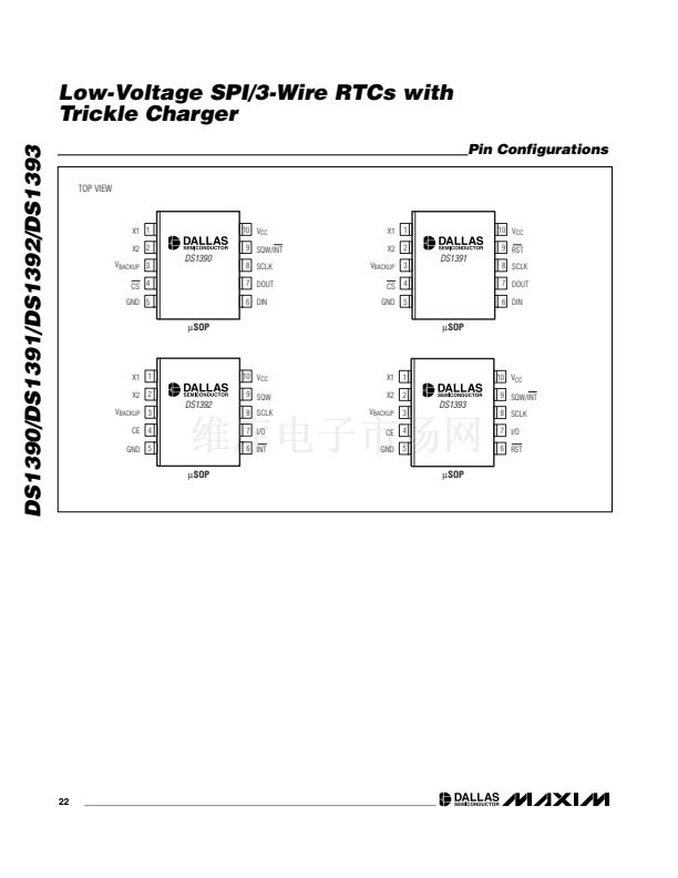
DS1390/DS1391/DS1392/DS1393
The INTCN bit used in the DS1390/DS1393 becomes
the SQW pin-enable bit in the DS1392. This bit powers
up a zero, making SQW active.
Status Register (0E/8Eh)
BIT 7
OSF
BIT 6
0
BIT 5
0
BIT 4
0
BIT 3
0
BIT 2
0
BIT 1
0
BIT 0
AF
Bit 7: Oscillator Stop Flag (OSF).
A logic 1 in this bit
indicates that the oscillator has stopped or was
stopped for some time and may be used to judge the
validity of the clock and calendar data. This bit is
edge-triggered and is set to logic 1 when the internal
circuitry senses the oscillator has transitioned from a
normal run state to a STOP condition. The following are
examples of conditions that can cause the OSF bit to
be set:
1) The first time power is applied.
2) The voltage present on V
CC
and V
BACKUP
is
insufficient to support oscillation.
3) The
EOSC
bit is turned off.
4) External influences on the crystal (i.e., noise,
leakage, etc.).
This bit remains at logic 1 until written to logic 0. This
bit can only be written to logic 0. Attempting to write
OSF to logic 1 leaves the value unchanged.
Bit 6: Alarm Flag (AF).
A logic 1 in the AF bit indicates
that the time matched the alarm registers. If the AIE bit
is logic 1 and the INTCN bit is set to logic 1, the
SQW/INT pin is also asserted. AF is cleared when writ-
ten to logic 0. This bit can only be written to logic 0.
Attempting to write to logic 1 leaves the value
unchanged.
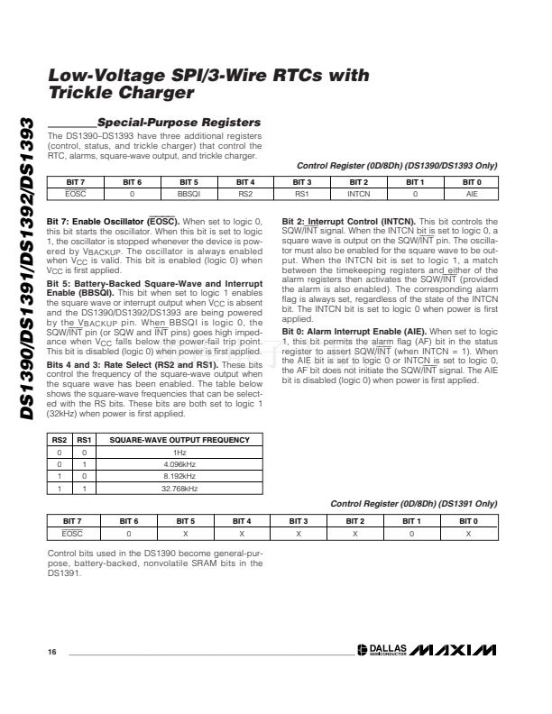
Trickle-Charge Register (0F/8Fh)
The simplified schematic in Figure 9 shows the basic
components of the trickle charger. The trickle-charge
select (TCS) bits (bits 4 to 7) control the selection of
the trickle charger. To prevent accidental enabling,
only a pattern on 1010 enables the trickle charger. All
other patterns disable the trickle charger. The trickle
charger is disabled when power is first applied. The
diode-select (DS) bits (bits 2 and 3) select whether or
not a diode is connected between V
CC
and V
BACKUP
.
If DS is 01, no diode is selected or if DS is 10, a diode
is selected. The ROUT bits (bits 0 and 1) select the
value of the resistor connected between V
CC
and
V
BACKUP
. Table 5 shows the resistor selected by the
resistor-select (ROUT) bits and the diode selected by
the diode-select (DS) bits.
Table 5. Trickle-Charge Register
TCS3
X
X
X
1
1
1
1
1
1
0
TCS2
X
X
X
0
0
0
0
0
0
0
TCS1
X
X
X
1
1
1
1
1
1
0
TCS0
X
X
X
0
0
0
0
0
0
0
DS1
0
1
X
0
1
0
1
0
1
0
DS0
0
1
X
1
0
1
0
1
0
0
ROUT1
X
X
0
0
0
1
1
1
1
0
ROUT0
X
X
0
1
1
0
0
1
1
0
Disabled
Disabled
Disabled
No diode, 250鈩?resistor
One diode, 250鈩?resistor
No diode, 2k鈩?resistor
One diode, 2k鈩?resistor
No diode, 4k鈩?resistor
One diode, 4k鈩?resistor
Initial default value鈥攄isabled
FUNCTION
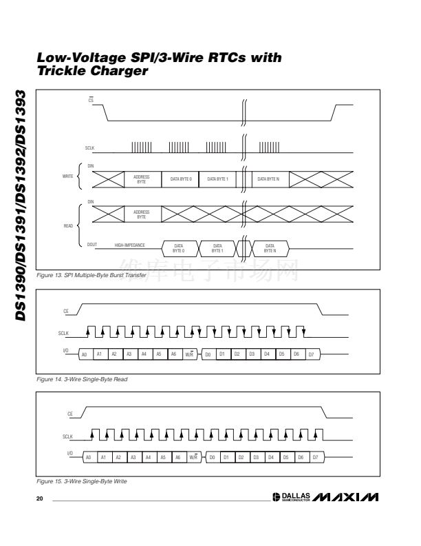
____________________________________________________________________
17


 1
1
 2
2
 3
3
 4
4
 5
5
 6
6
 7
7
 8
8
 9
9
 10
10
 11
11
 12
12
 13
13
 14
14
 15
15
 16
16
 17
17
 18
18
 19
19
 20
20
 21
21
 22
22
 23
23
 24
24
